- 您現(xiàn)在的位置:買賣IC網(wǎng) > PDF目錄362018 > A40MX04-2PL44I Field Programmable Gate Array (FPGA) PDF資料下載
參數(shù)資料
| 型號: | A40MX04-2PL44I |
| 英文描述: | Field Programmable Gate Array (FPGA) |
| 中文描述: | 現(xiàn)場可編程門陣列(FPGA) |
| 文件頁數(shù): | 9/116頁 |
| 文件大小: | 3110K |
| 代理商: | A40MX04-2PL44I |
第1頁第2頁第3頁第4頁第5頁第6頁第7頁第8頁當(dāng)前第9頁第10頁第11頁第12頁第13頁第14頁第15頁第16頁第17頁第18頁第19頁第20頁第21頁第22頁第23頁第24頁第25頁第26頁第27頁第28頁第29頁第30頁第31頁第32頁第33頁第34頁第35頁第36頁第37頁第38頁第39頁第40頁第41頁第42頁第43頁第44頁第45頁第46頁第47頁第48頁第49頁第50頁第51頁第52頁第53頁第54頁第55頁第56頁第57頁第58頁第59頁第60頁第61頁第62頁第63頁第64頁第65頁第66頁第67頁第68頁第69頁第70頁第71頁第72頁第73頁第74頁第75頁第76頁第77頁第78頁第79頁第80頁第81頁第82頁第83頁第84頁第85頁第86頁第87頁第88頁第89頁第90頁第91頁第92頁第93頁第94頁第95頁第96頁第97頁第98頁第99頁第100頁第101頁第102頁第103頁第104頁第105頁第106頁第107頁第108頁第109頁第110頁第111頁第112頁第113頁第114頁第115頁第116頁
v5.0
9
40MX and 42MX FPGA Families
routing. Each output segment spans four channels (two
above and two below), except near the top and bottom of
the array, where edge effects occur. Long vertical tracks
contain either one or two segments. An example of vertical
routing tracks and segments is shown in
Figure 8
.
Antifuse Structures
An antifuse is a
“
normally open
”
structure as opposed to the
normally connected fuse structure used in PROMs or PALs.
The use of antifuses to implement a programmable logic
device results in highly testable structures as well as
efficient programming algorithms. The structure is
highly-testable because there are no pre-existing
connections; therefore, temporary connections can be made
using pass transistors. These temporary connections can
isolate individual antifuses to be programmed and
individual circuit structures to be tested, which can be done
before and after programming. For example, all metal
tracks can be tested for continuity and shorts between
adjacent tracks, and the functionality of all logic modules
can be verified.
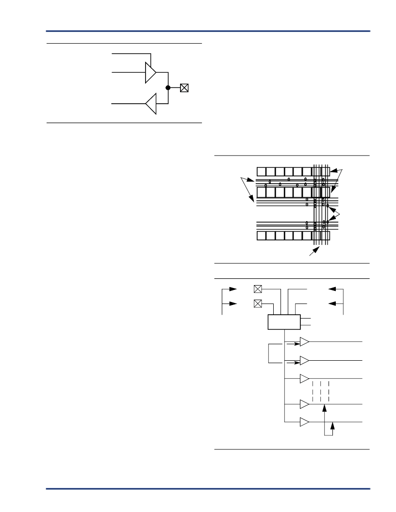
Clock Networks
The 40MX devices have one global clock distribution
network (CLK). Two low-skew, high-fanout clock
distribution networks are provided in each 42MX device.
These networks are referred to as
CLK0
and
CLK1
. Each
network has a clock module (CLKMOD) that selects the
source of the clock signal and may be driven as follows:
Externally from the CLKA pad
Externally from the CLKB pad
Internally from the CLKINTA input
Internally from the CLKINTB input
The clock modules are located in the top row of I/O
modules. Clock drivers and a dedicated horizontal clock
track are located in each horizontal routing channel.
The user controls the clock module by selecting one of two
clock macros from the macro library. The macro CLKBUF is
used to connect one of the two external clock pins to a clock
network, and the macro CLKINT is used to connect an
internally-generated clock signal to a clock network. Since
both clock networks are identical, it does not matter
whether CLK0 or CLK1 is being used. The clock input pads
can also be used as normal I/Os, bypassing the clock
networks (
Figure 9
).
The A42MX36 device has four additional register control
resources, called quadrant clock networks (
Figure 10 on
page 10
). Each quadrant clock provides a local, high-fanout
resource to the contiguous logic modules within its
quadrant of the device. Quadrant clock signals can originate
from specific I/O pins or from the internal array and can be
used as a secondary register clock, register clear, or output
enable.
Figure 7
40MX I/O Module
OE
From Internal Logic
To Internal Logic
Figure 8
Routing Structure
Figure 9
Clock Networks
Vertical Routing Tracks
Antifuses
Logic
Modules
Segmented
Horizontal
Routing
Tracks
CLKB
CLKA
From
Pads
Clock
Drivers
CLKMOD
CLKINB
CLKINA
S0
S1
Internal
Signal
CLKO(17)
CLKO(16)
CLKO(15)
CLKO(2)
CLKO(1)
Clock Tracks
相關(guān)PDF資料 |
PDF描述 |
|---|---|
| A40MX04-2PL44M | Field Programmable Gate Array (FPGA) |
| A40MX04-2PL68 | Field Programmable Gate Array (FPGA) |
| A40MX04-2PL68I | Field Programmable Gate Array (FPGA) |
| A40MX04-2PL68M | Field Programmable Gate Array (FPGA) |
| A40MX04-2PL84 | Field Programmable Gate Array (FPGA) |
相關(guān)代理商/技術(shù)參數(shù) |
參數(shù)描述 |
|---|---|
| A40MX04-2PL44M | 制造商:未知廠家 制造商全稱:未知廠家 功能描述:Field Programmable Gate Array (FPGA) |
| A40MX04-2PL68 | 功能描述:IC FPGA MX SGL CHIP 6K 68-PLCC RoHS:否 類別:集成電路 (IC) >> 嵌入式 - FPGA(現(xiàn)場可編程門陣列) 系列:MX 標(biāo)準(zhǔn)包裝:90 系列:ProASIC3 LAB/CLB數(shù):- 邏輯元件/單元數(shù):- RAM 位總計(jì):36864 輸入/輸出數(shù):157 門數(shù):250000 電源電壓:1.425 V ~ 1.575 V 安裝類型:表面貼裝 工作溫度:-40°C ~ 125°C 封裝/外殼:256-LBGA 供應(yīng)商設(shè)備封裝:256-FPBGA(17x17) |
| A40MX04-2PL68I | 功能描述:IC FPGA MX SGL CHIP 6K 68-PLCC RoHS:否 類別:集成電路 (IC) >> 嵌入式 - FPGA(現(xiàn)場可編程門陣列) 系列:MX 標(biāo)準(zhǔn)包裝:90 系列:ProASIC3 LAB/CLB數(shù):- 邏輯元件/單元數(shù):- RAM 位總計(jì):36864 輸入/輸出數(shù):157 門數(shù):250000 電源電壓:1.425 V ~ 1.575 V 安裝類型:表面貼裝 工作溫度:-40°C ~ 125°C 封裝/外殼:256-LBGA 供應(yīng)商設(shè)備封裝:256-FPBGA(17x17) |
| A40MX04-2PL68M | 制造商:未知廠家 制造商全稱:未知廠家 功能描述:Field Programmable Gate Array (FPGA) |
| A40MX04-2PL84 | 功能描述:IC FPGA MX SGL CHIP 6K 84-PLCC RoHS:否 類別:集成電路 (IC) >> 嵌入式 - FPGA(現(xiàn)場可編程門陣列) 系列:MX 標(biāo)準(zhǔn)包裝:90 系列:ProASIC3 LAB/CLB數(shù):- 邏輯元件/單元數(shù):- RAM 位總計(jì):36864 輸入/輸出數(shù):157 門數(shù):250000 電源電壓:1.425 V ~ 1.575 V 安裝類型:表面貼裝 工作溫度:-40°C ~ 125°C 封裝/外殼:256-LBGA 供應(yīng)商設(shè)備封裝:256-FPBGA(17x17) |
發(fā)布緊急采購,3分鐘左右您將得到回復(fù)。