- 您現(xiàn)在的位置:買賣IC網(wǎng) > PDF目錄360656 > 9S12DT128BDGV1 9S12DT128B Device Guide PDF資料下載
參數(shù)資料
| 型號: | 9S12DT128BDGV1 |
| 英文描述: | 9S12DT128B Device Guide |
| 中文描述: | 9S12DT128B設(shè)備指南 |
| 文件頁數(shù): | 106/126頁 |
| 文件大小: | 1809K |
| 代理商: | 9S12DT128BDGV1 |
第1頁第2頁第3頁第4頁第5頁第6頁第7頁第8頁第9頁第10頁第11頁第12頁第13頁第14頁第15頁第16頁第17頁第18頁第19頁第20頁第21頁第22頁第23頁第24頁第25頁第26頁第27頁第28頁第29頁第30頁第31頁第32頁第33頁第34頁第35頁第36頁第37頁第38頁第39頁第40頁第41頁第42頁第43頁第44頁第45頁第46頁第47頁第48頁第49頁第50頁第51頁第52頁第53頁第54頁第55頁第56頁第57頁第58頁第59頁第60頁第61頁第62頁第63頁第64頁第65頁第66頁第67頁第68頁第69頁第70頁第71頁第72頁第73頁第74頁第75頁第76頁第77頁第78頁第79頁第80頁第81頁第82頁第83頁第84頁第85頁第86頁第87頁第88頁第89頁第90頁第91頁第92頁第93頁第94頁第95頁第96頁第97頁第98頁第99頁第100頁第101頁第102頁第103頁第104頁第105頁當(dāng)前第106頁第107頁第108頁第109頁第110頁第111頁第112頁第113頁第114頁第115頁第116頁第117頁第118頁第119頁第120頁第121頁第122頁第123頁第124頁第125頁第126頁
MC9S12DJ64 Device User Guide — V01.17
106
A.5.1.5 Pseudo Stop and Wait Recovery
The recovery from Pseudo STOP and Wait are essentially the same since the oscillator was not stopped in
both modes. The controller can be woken up by internal or external interrupts. After t
wrs
the CPU starts
fetching the interrupt vector.
A.5.2 Oscillator
The device features an internal Colpitts and Pierce oscillator. The selection of Colpitts oscillator or Pierce
oscillator/external clock depends on the XCLKS signal which is sampled during reset. Pierce
oscillator/external clock mode allows the input of a square wave. Before asserting the oscillator to the
internal system clocks the quality of the oscillation is checked for each start from either power-on, STOP
oroscillatorfail.t
CQOUT
specifiesthemaximumtimebeforeswitchingtotheinternalselfclockmodeafter
POR or STOP if a proper oscillation is not detected. The quality check also determines the minimum
oscillator start-up time t
UPOSC
. The device also features a clock monitor. A Clock Monitor Failure is
asserted if the frequency of the incoming clock signal is below the Assert Frequency f
CMFA.
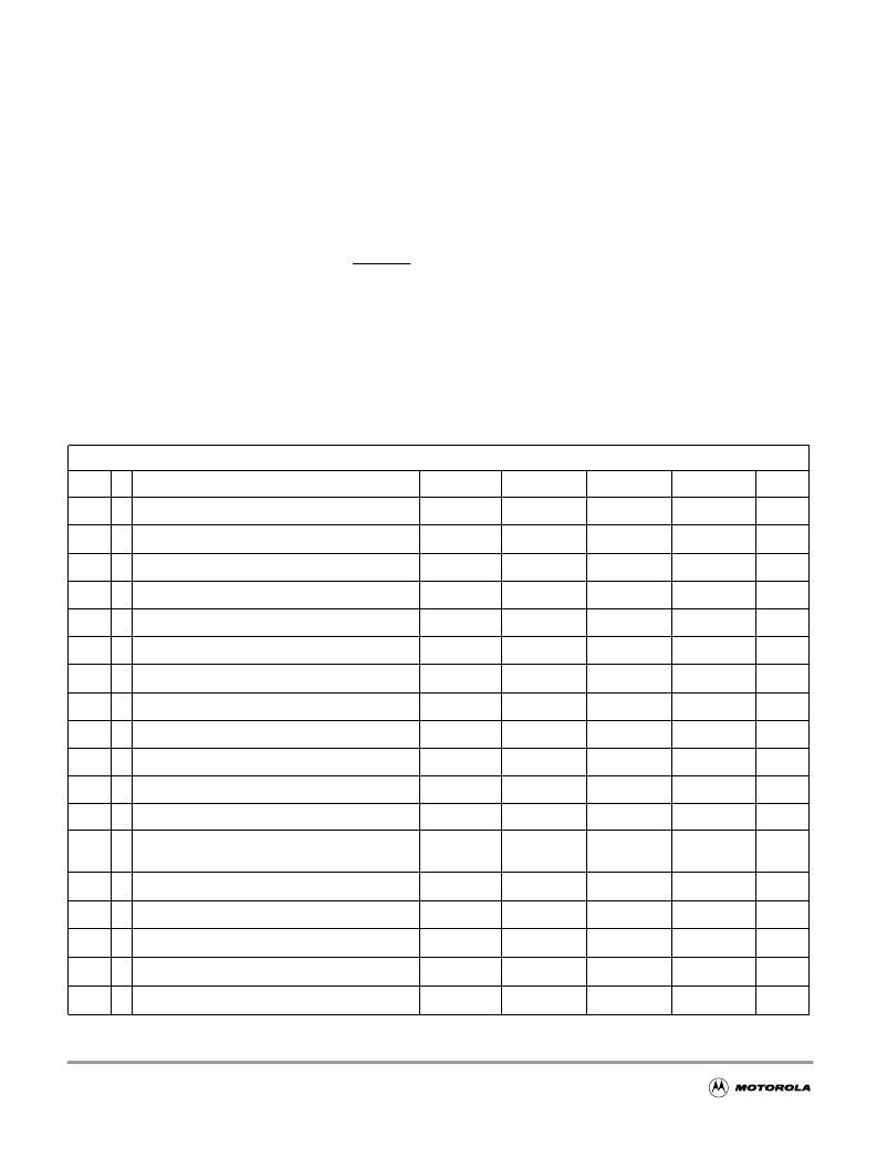
Table A-15 Oscillator Characteristics
Conditions are shown in
Table A-4
unless otherwise noted
Num C
Rating
Symbol
Min
Typ
Max
Unit
1a
C Crystal oscillator range (Colpitts)
f
OSC
0.5
16
MHz
1b
C Crystal oscillator range (Pierce)
1
f
OSC
0.5
40
MHz
2
P Startup Current
i
OSC
100
μ
A
3
C Oscillator start-up time (Colpitts)
t
UPOSC
8
2
100
3
ms
4
D Clock Quality check time-out
t
CQOUT
0.45
2.5
s
5
P Clock Monitor Failure Assert Frequency
f
CMFA
50
100
200
KHz
6
P External square wave input frequency
4
f
EXT
0.5
50
MHz
7
D External square wave pulse width low
t
EXTL
9.5
ns
8
D External square wave pulse width high
t
EXTH
9.5
ns
9
D External square wave rise time
t
EXTR
1
ns
10
D External square wave fall time
t
EXTF
1
ns
11
D Input Capacitance (EXTAL, XTAL pins)
C
IN
7
pF
12
C
DC Operating Bias in Colpitts Configuration on
EXTAL Pin
V
DCBIAS
1.1
V
13
P EXTAL Pin Input High Voltage
4
V
IH,EXTAL
0.7*V
DDPLL
V
T EXTAL Pin Input High Voltage
4
V
IH,EXTAL
V
DDPLL
+ 0.3
V
14
P EXTAL Pin Input Low Voltage
4
V
IL,EXTAL
0.3*V
DDPLL
V
T EXTAL Pin Input Low Voltage
4
V
IL,EXTAL
V
DDPLL
- 0.3
V
15
C EXTAL Pin Input Hysteresis
4
V
HYS,EXTAL
250
mV
相關(guān)PDF資料 |
PDF描述 |
|---|---|
| 9S12DT128DGV2 | MC9S12DT128 Device User Guide V02.09 |
| 9S12DT128DGV2D | MC9S12DT128 Device User Guide V02.09 |
| 9S12DT256DGV3 | MC9S12DT256 Device User Guide V03.03 |
| 9S12E128DGV1 | MC9S12E-Family Device User Guide V01.04 |
| 9S12H128 | 16-bit Microcontroller |
相關(guān)代理商/技術(shù)參數(shù) |
參數(shù)描述 |
|---|---|
| 9S12DT128DGV2 | 制造商:MOTOROLA 制造商全稱:Motorola, Inc 功能描述:MC9S12DT128 Device User Guide V02.09 |
| 9S12DT128DGV2D | 制造商:MOTOROLA 制造商全稱:Motorola, Inc 功能描述:MC9S12DT128 Device User Guide V02.09 |
| 9S12DT256DGV3 | 制造商:MOTOROLA 制造商全稱:Motorola, Inc 功能描述:MC9S12DT256 Device User Guide V03.03 |
| 9S12E128DGV1 | 制造商:MOTOROLA 制造商全稱:Motorola, Inc 功能描述:MC9S12E-Family Device User Guide V01.04 |
| 9S12H128 | 制造商:FREESCALE 制造商全稱:Freescale Semiconductor, Inc 功能描述:16-bit Microcontroller |
發(fā)布緊急采購,3分鐘左右您將得到回復(fù)。