- 您現(xiàn)在的位置:買賣IC網(wǎng) > PDF目錄25570 > 9LPRS501YKLFT (INTEGRATED DEVICE TECHNOLOGY INC) SPECIALTY MICROPROCESSOR CIRCUIT, PQCC64 PDF資料下載
參數(shù)資料
| 型號: | 9LPRS501YKLFT |
| 廠商: | INTEGRATED DEVICE TECHNOLOGY INC |
| 元件分類: | 微控制器/微處理器 |
| 英文描述: | SPECIALTY MICROPROCESSOR CIRCUIT, PQCC64 |
| 封裝: | ROHS COMPLIANT, PLASTIC, MLF-64 |
| 文件頁數(shù): | 23/28頁 |
| 文件大小: | 265K |
| 代理商: | 9LPRS501YKLFT |
第1頁第2頁第3頁第4頁第5頁第6頁第7頁第8頁第9頁第10頁第11頁第12頁第13頁第14頁第15頁第16頁第17頁第18頁第19頁第20頁第21頁第22頁當前第23頁第24頁第25頁第26頁第27頁第28頁
IDTTM/ICSTM
64-pin CK505 w/Fully Integrated Voltage Regulator + Integrated Series Resistor
1121F—02/23/09
Advance Information
ICS9LPRS501
64-PIN CK505 W/FULLY INTEGRATED VOLTAGE REGULATOR + INTEGRATED SERIES RESISTOR
4
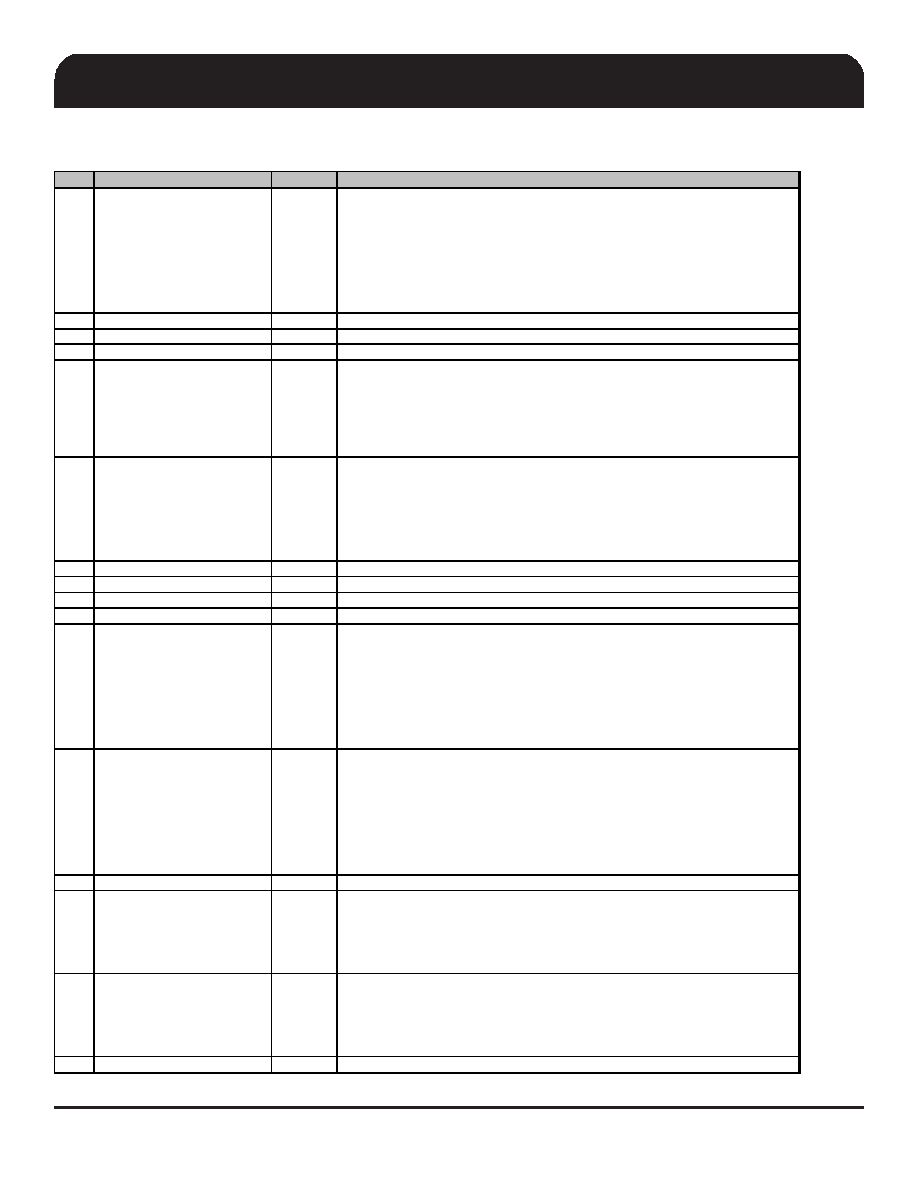
TSSOP Pin Description (Continued)
PIN #
PIN NAME
TYPE
DESCRIPTION
33
SRCT11/CR#_H
I/O
SRC11 true or Clock Request control H for SRC10 pair
The power-up default is SRC11, but this pin may also be used as a Clock Request control of
SRC10 via SMBus. Before configuring this pin as a Clock Request Pin, the SRC11 output pair
must first be disabled in byte 3 bit 7 of SMBus configuration space After the SRC11 output is
disabled (high-Z), the pin can then be set to serve as a Clock Request for SRC10 pair using
byte 6, bit 4 of SMBus configuration space
Byte 6, bit 4
0 = SRC11 enabled (default)
1= CR#_H controls SRC10.
34
SRCT10
OUT
True clock of differential SRC clock pair.
35
SRCC10
OUT
Cpmplement clock of differential SRC clock pair.
36
VDDSRC_IO
PWR
Power supply for SRC outputs. VDDSRC_IO is 1.05 to 3.3V with +/-5% tolerance
37
CPU_STOP#/SRCC5
I/O
Stops all CPU Clocks, except those set to be free running clocks /
Complement clock of differential SRC pair. The function of this pin is set up by the power-up
strap on pin 6, PCI4/SRC5_EN. The logic value sampled on pin 6 at power-up sets the function
as follows:
0= CPU_STOP#
1 = SRC5
In AMT mode 3 bits are shifted in from the ICH to set the FSC, FSB, FSA values
38
PCI_STOP#/SRCT5
I/O
Stops all PCI Clocks, except those set to be free running clocks /
Complement clock of differential SRC pair. The function of this pin is set up by the power-up
strap on pin 6, PCI4/SRC5_EN. The logic value sampled on pin 6 at power-up sets the function
as follows:
0= PCI_STOP#
1 = SRC5#
In AMT mode, this pin is a clock input which times the FSC, FSB, FSA bits shifted in on pin 37.
39
VDDSRC
PWR
VDD pin for SRC internal circuits, 3.3V nominal
40
SRCC6
OUT
Complement clock of low power differential SRC clock pair.
41
SRCT6
OUT
True clock of low power differential SRC clock pair.
42
GNDSRC
PWR
Ground for SRC clocks
43
SRCC7/CR#_E
I/O
SRC7 complement or Clock Request control E for SRC6 pair
The power-up default is SRC7#, but this pin may also be used as a Clock Request control of
SRC6 via SMBus. Before configuring this pin as a Clock Request Pin, the SRC7 output pair
must first be disabled in byte 3, bit 3 of SMBus configuration space . After the SRC output is
disabled (high-Z), the pin can then be set to serve as a Clock Request for SRC6 pair using byte
6, bit 7 of SMBus configuration space
Byte 6, bit 7
0 = SRC7# enabled (default)
1= CR#_E controls SRC6.
44
SRCT7/CR#_F
I/O
SRC7 true or Clock Request control 8 for SRC8 pair
The power-up default is SRC7, but this pin may also be used as a Clock Request control of
SRC8 via SMBus. Before configuring this pin as a Clock Request Pin, the SRC7 output pair
must first be disabled in byte 3, bit 3 of SMBus configuration space After the SRC output is
disabled (high-Z), the pin can then be set to serve as a Clock Request for SRC8 pair using byte
6, bit 6 of SMBus configuration space
Byte 6, bit 6
0 = SRC7# enabled (default)
1 = CR#_F controls SRC8.
45
VDDSRC_IO
PWR
Power supply for SRC outputs. VDDSRC_IO is 1.05 to 3.3V with +/-5% tolerance
46
CPUC2_ITP/SRCC8
OUT
Complement clock of low power differential CPU2/Complement clock of differential SRC pair.
The function of this pin is determined by the latched input value on pin 7, PCIF5/ITP_EN on
powerup. The function is as follows:
Pin 7 latched input Value
0 = SRC8#
1 = ITP#
47
CPUT2_ITP/SRCT8
OUT
True clock of low power differential CPU2/True clock of differential SRC pair. The function of this
pin is determined by the latched input value on pin 7, PCIF5/ITP_EN on powerup. The function is
as follows:
Pin 7 latched input Value
0 = SRC8
1 = ITP
48
NC
N/A
No Connect
相關(guān)PDF資料 |
PDF描述 |
|---|---|
| 9LPRS502YFLFT | SPECIALTY MICROPROCESSOR CIRCUIT, PDSO56 |
| 9LPRS502YGLFT | SPECIALTY MICROPROCESSOR CIRCUIT, PDSO56 |
| 9LPRS502YKLFT | SPECIALTY MICROPROCESSOR CIRCUIT, PQCC56 |
| 9LPRS511EGLF | SPECIALTY MICROPROCESSOR CIRCUIT, PDSO64 |
| 9LPRS525AFLFT | SPECIALTY MICROPROCESSOR CIRCUIT, PDSO56 |
相關(guān)代理商/技術(shù)參數(shù) |
參數(shù)描述 |
|---|---|
| 9LPRS502HGLF | 制造商:Integrated Device Technology Inc 功能描述:IDT 9LPRS502HGLF LOGIC AND TIMING MISC - Rail/Tube 制造商:Integrated Device Technology Inc 功能描述:IDT 9LPRS502HGLF Logic and Timing Misc |
| 9LPRS502PGLF | 制造商:Integrated Device Technology Inc 功能描述:IDT 9LPRS502PGLF PHASED LOCKED LOOP (PLL) - Rail/Tube 制造商:Integrated Device Technology Inc 功能描述:IDT 9LPRS502PGLF Phased Locked Loop (PLL) |
| 9LPRS502SFLF | 功能描述:時鐘合成器/抖動清除器 RoHS:否 制造商:Skyworks Solutions, Inc. 輸出端數(shù)量: 輸出電平: 最大輸出頻率: 輸入電平: 最大輸入頻率:6.1 GHz 電源電壓-最大:3.3 V 電源電壓-最小:2.7 V 封裝 / 箱體:TSSOP-28 封裝:Reel |
| 9LPRS502SFLFT | 功能描述:時鐘合成器/抖動清除器 RoHS:否 制造商:Skyworks Solutions, Inc. 輸出端數(shù)量: 輸出電平: 最大輸出頻率: 輸入電平: 最大輸入頻率:6.1 GHz 電源電壓-最大:3.3 V 電源電壓-最小:2.7 V 封裝 / 箱體:TSSOP-28 封裝:Reel |
| 9LPRS502SGLF | 功能描述:時鐘合成器/抖動清除器 RoHS:否 制造商:Skyworks Solutions, Inc. 輸出端數(shù)量: 輸出電平: 最大輸出頻率: 輸入電平: 最大輸入頻率:6.1 GHz 電源電壓-最大:3.3 V 電源電壓-最小:2.7 V 封裝 / 箱體:TSSOP-28 封裝:Reel |
發(fā)布緊急采購,3分鐘左右您將得到回復。