- 您現(xiàn)在的位置:買賣IC網(wǎng) > PDF目錄42522 > 97632-11 (PEREGRINE SEMICONDUCTOR CORP) PLL FREQUENCY SYNTHESIZER, 300 MHz, CQCC68 PDF資料下載
參數(shù)資料
| 型號: | 97632-11 |
| 廠商: | PEREGRINE SEMICONDUCTOR CORP |
| 元件分類: | PLL合成/DDS/VCOs |
| 英文描述: | PLL FREQUENCY SYNTHESIZER, 300 MHz, CQCC68 |
| 封裝: | CERAMIC, QFJ-68 |
| 文件頁數(shù): | 3/16頁 |
| 文件大小: | 677K |
| 代理商: | 97632-11 |
Product Specification
PE97632
Page 11 of 16
2006-2010 Peregrine Semiconductor Corp. All rights reserved.
Document No. 70-0205-06
│ UltraCMOS RFIC Solutions
While the E_WR input is “high” and the S_WR
input is “l(fā)ow”, serial input data (Sdata input), B0 to
B7, are clocked serially into the enhancement
register on the rising edge of Sclk, MSB (B0) first.
The enhancement register is double buffered to
prevent inadvertent control changes during serial
loading, with buffer capture of the serially entered
data performed on the falling edge of E_WR
according to the timing diagram shown in
Figure 7. After the falling edge of E_WR, the data
provide control bits as shown in Table 9 on page
10 will have their bit functionality enabled by
asserting the Enh input “l(fā)ow”.
Direct Interface Mode
Direct Interface Mode is selected by setting the
“Direct” input “high”.
Counter control bits are set directly at the pins as
shown in Table 7 and Table 8.
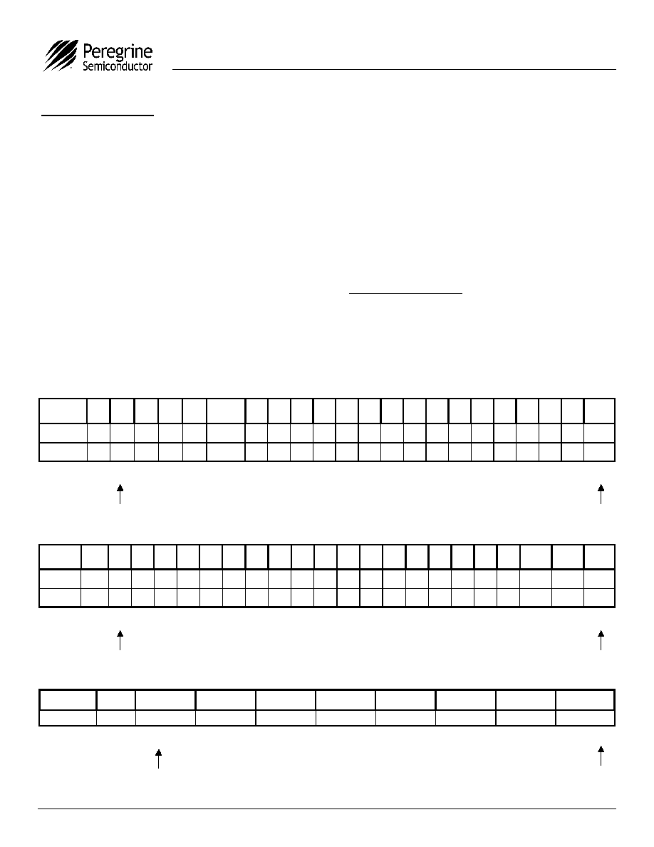
Table 7. Secondary Register Programming
Table 8. Auxiliary Register Programming
Table 9. Enhancement Register Programming
Interface
Mode
E
En
n
nh
h
R5
R4
M8
M7
Pr
Preeee_e
_e
_en
n
M6
M5
M4
M3
M2
M1
M0
R3
R2
R1
R0
A3
A2
A1
A0
Addr
Direct
1
R5
R4
M8
M7
Pre_en
M6
M5
M4
M3
M2
M1
M0
R3
R2
R1
R0
A3
A2
A1
A0
X
Serial*
1
B0
B1
B2
B3
B4
B5
B6
B7
B8
B9
B10
B11
B12
B13
B14
B15
B16
B17
B18
B19
0
*Serial data clocked serially on Sclk rising edge while E_WR “l(fā)ow” and captured in secondary register on S_WR rising edge.
Interface
Mode
E
En
n
nh
h
K17
K16
K15
K14
K13
K12
K11
K10
K9
K8
K7
K6
K5
K4
K3
K2
K1
K0
Rsrv
Addr
Direct
1
K17
K16
K15
K14
K13
K12
K11
K10
K9
K8
K7
K6
K5
K4
K3
K2
K1
K0
X
Serial*
1
B0
B1
B2
B3
B4
B5
B6
B7
B8
B9
B10
B11
B12
B13
B14
B15
B16
B17
B18
B19
1
*Serial data clocked serially on Sclk rising edge while E_WR “l(fā)ow” and captured in secondary register on S_WR rising edge.
Interface
Mode
En
Enh
h
Reserved
fp output
Power
Down
Counter
load
MSEL
output
fc output
LD Disable
Serial*
0
B0
B1
B2
B3
B4
B5
B6
B7
*Serial data clocked serially on Sclk rising edge while E_WR “high” and captured in the double buffer on E_WR falling edge.
MSB (first in)
(last in) LSB
MSB (first in)
Register Programming
Serial Interface Mode
While the E_WR input is “l(fā)ow” and the S_WR input
is “l(fā)ow”, serial input data (Sdata input), B0 to B20,
are clocked serially into the primary register on the
rising edge of Sclk, MSB (B0) first. The LSB is
used as an address bit. When “0”, the contents
from the primary register are transferred into the
secondary register on the rising edge of either
S_WR according to the timing diagrams shown in
Figure 7. When “1”, data is transferred to the
auxiliary register according to the same timing
diagram. The secondary register is used to
program the various counters, while the auxiliary
register is used to program the DSM.
Data are transferred to the counters as shown in
Table 8.
相關(guān)PDF資料 |
PDF描述 |
|---|---|
| 9764-025-HA | INTERCONNECTION DEVICE |
| 7308-001 | INTERCONNECTION DEVICE |
| 7308 | INTERCONNECTION DEVICE |
| 7213 | INTERCONNECTION DEVICE |
| 9764-028 | INTERCONNECTION DEVICE |
相關(guān)代理商/技術(shù)參數(shù) |
參數(shù)描述 |
|---|---|
| 97633 | 制造商:未知廠家 制造商全稱:未知廠家 功能描述:KUPPLUNG BNC 75 OHM RG59 BLAU |
| 97633A360 | 制造商:MISC. COMMERCIAL HRD 功能描述: |
| 9763602028 | 制造商:Laird Technologies Inc 功能描述:NOSG,STR,BF,CLO,CTL/.104x.357x.188x2.802 |
| 9763602081 | 制造商:Laird Technologies Inc 功能描述:NOSG,STR,BF,CLO,CTL / .104X.357X.188X8.066 / UOM=EA |
| 9763-A-1032-0 | 制造商:Amatom Electronic Hardware 功能描述: |
發(fā)布緊急采購,3分鐘左右您將得到回復(fù)。