- 您現(xiàn)在的位置:買賣IC網(wǎng) > PDF目錄42522 > 97632-11 (PEREGRINE SEMICONDUCTOR CORP) PLL FREQUENCY SYNTHESIZER, 300 MHz, CQCC68 PDF資料下載
參數(shù)資料
| 型號: | 97632-11 |
| 廠商: | PEREGRINE SEMICONDUCTOR CORP |
| 元件分類: | PLL合成/DDS/VCOs |
| 英文描述: | PLL FREQUENCY SYNTHESIZER, 300 MHz, CQCC68 |
| 封裝: | CERAMIC, QFJ-68 |
| 文件頁數(shù): | 14/16頁 |
| 文件大小: | 677K |
| 代理商: | 97632-11 |
Product Specification
PE97632
Document No. 70-0205-06
│ www.psemi.com
2006-2010 Peregrine Semiconductor Corp. All rights reserved.
Page 7 of 16
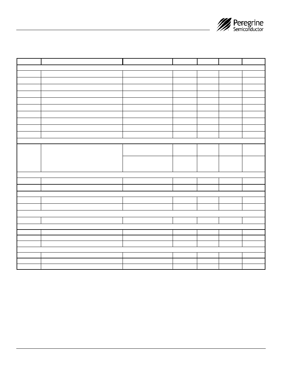
Table 6. AC Characteristics
VDD = 3.30 V -40°C < TA < 85°C, Unless otherwise specified
Note 1:
fclk is verified during the functional pattern test. Serial programming sections of the functional pattern are clocked at 10 MHz to verify fclk
specification.
Note 2:
CMOS logic levels can be used to drive reference input if DC coupled. For Sin wave inputs, amplitude needs to be a minimum of 0.5 Vp-p
with no maximum level specified.
Note 3:
Parameter is guaranteed through characterization only and is not tested.
Note 4:
Parameter below are not tested for die sales. These parameters are verified during the element
Symbol
Parameter
Conditions
Min
Typ
Max
Units
Control Interface and Latches (see Figures 6, 7)
fClk
Serial data clock frequency
(Note 1)
10
MHz
tClkH
Serial clock HIGH time
30
ns
tClkL
Serial clock LOW time
30
ns
tDSU
Sdata set-up time to Sclk rising edge
10
ns
tDHLD
Sdata hold time after Sclk rising edge
10
ns
tPW
S_WR pulse width
30
ns
tCWR
Sclk rising edge to S_WR rising edge
30
ns
tCE
Sclk falling edge to E_WR transition
30
ns
tWRC
S_WR falling edge to Sclk rising edge
30
ns
tEC
E_WR transition to Sclk rising edge
30
ns
Main Divider (Prescaler Enabled) (Note 4)
PFin
Input level range
External AC coupling
275 MHz
≤ Freq ≤ 3200MHz
-5
5
dBm
External AC coupling
3.2 GHz < Freq
≤ 3.5 GHz
3.15 V
≤ VDD ≤ 3.45 V
0
5
dBm
Main Divider (Prescaler Bypassed) (Note 4)
Fin
Operating frequency
50
300
MHz
PFin
Input level range
External AC coupling
-5
5
dBm
Reference Divider
fr
Operating frequency
(Note 3)
100
MHz
Pfr
Reference input power (Note 2)
Single ended input
-2
dBm
Phase Detector
fc
Comparison frequency
(Note 3)
50
MHz
SSB Phase Noise (Fin = 1.9 GHz, fr = 20 MHz, fc = 20 MHz, LBW = 50 kHz, VDD = 3.3 V, Temp = 25° C) (Note 4)
ΦN
Phase Noise
100 Hz Offset
-89
dBc/Hz
ΦN
Phase Noise
1 kHz Offset
-96
dBc/Hz
ΦN
Phase Noise
10 kHz Offset
-101
dBc/Hz
SSB Phase Noise (Fin = 1.9 GHz, fr = 20 MHz, fc = 20 MHz, LBW = 50 kHz, VDD = 3.0 V, Temp = 25° C) (Note 4)
ΦN
Phase Noise
100 Hz Offset
-84
dBc/Hz
ΦN
Phase Noise
1 kHz Offset
-92
dBc/Hz
ΦN
Phase Noise
10 kHz Offset
-100
dBc/Hz
相關(guān)PDF資料 |
PDF描述 |
|---|---|
| 9764-025-HA | INTERCONNECTION DEVICE |
| 7308-001 | INTERCONNECTION DEVICE |
| 7308 | INTERCONNECTION DEVICE |
| 7213 | INTERCONNECTION DEVICE |
| 9764-028 | INTERCONNECTION DEVICE |
相關(guān)代理商/技術(shù)參數(shù) |
參數(shù)描述 |
|---|---|
| 97633 | 制造商:未知廠家 制造商全稱:未知廠家 功能描述:KUPPLUNG BNC 75 OHM RG59 BLAU |
| 97633A360 | 制造商:MISC. COMMERCIAL HRD 功能描述: |
| 9763602028 | 制造商:Laird Technologies Inc 功能描述:NOSG,STR,BF,CLO,CTL/.104x.357x.188x2.802 |
| 9763602081 | 制造商:Laird Technologies Inc 功能描述:NOSG,STR,BF,CLO,CTL / .104X.357X.188X8.066 / UOM=EA |
| 9763-A-1032-0 | 制造商:Amatom Electronic Hardware 功能描述: |
發(fā)布緊急采購,3分鐘左右您將得到回復(fù)。