- 您現(xiàn)在的位置:買(mǎi)賣(mài)IC網(wǎng) > PDF目錄24813 > 935264405118 (NXP SEMICONDUCTORS) PLL BASED CLOCK DRIVER, 10 TRUE OUTPUT(S), 0 INVERTED OUTPUT(S), PDSO24 PDF資料下載
參數(shù)資料
| 型號(hào): | 935264405118 |
| 廠商: | NXP SEMICONDUCTORS |
| 元件分類: | 時(shí)鐘及定時(shí) |
| 英文描述: | PLL BASED CLOCK DRIVER, 10 TRUE OUTPUT(S), 0 INVERTED OUTPUT(S), PDSO24 |
| 封裝: | 4.40 MM, PLASTIC, MO-153, SOT-355-1, TSSOP-24 |
| 文件頁(yè)數(shù): | 7/10頁(yè) |
| 文件大?。?/td> | 95K |
| 代理商: | 935264405118 |

Philips Semiconductors
Product specification
PCK2510S
50–150 MHz 1:10 SDRAM clock driver
2001 Feb 02
6
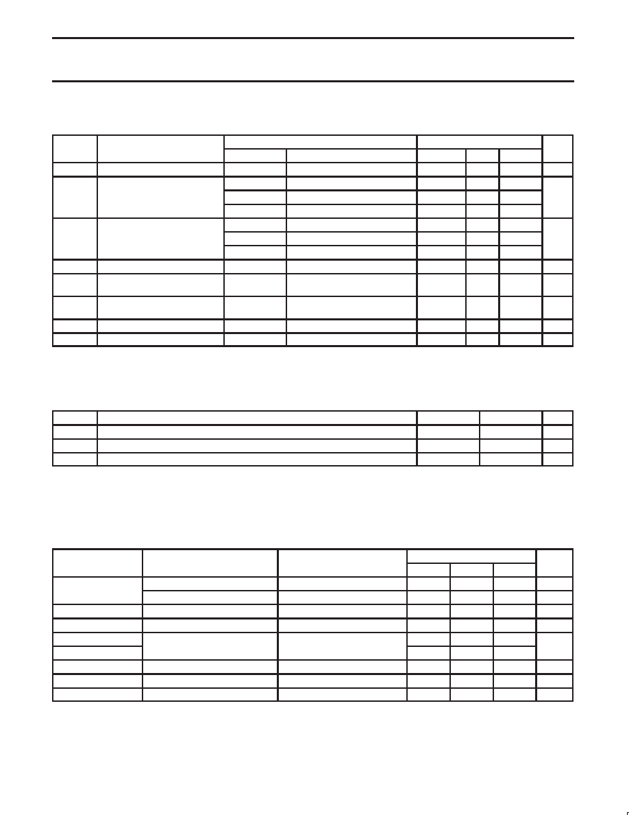
ELECTRICAL CHARACTERISTICS
Over recommended operating free-air temperature range (unless otherwise noted)
SYMBOL
PARAMETER
TEST CONDITIONS
LIMITS
UNIT
SYMBOL
PARAMETER
AVCC, VCC (V)
OTHER
MIN
TYP
MAX
UNIT
VIK
Input clamp voltage
3
II = –18 mA
–1.2
V
MIN to MAX
IOH = – 100 A
VCC – 0.2
VOH
HIGH level output voltage
3
IOH = – 12 mA
2.1
V
3
IOH = – 6 mA
2.4
MIN to MAX
IOL = 100 A
–
0.2
VOL
LOW level output voltage
3
IOL = 12 mA
–
0.8
V
3
IOL = 6 mA
–
0.55
II
Input current
3.6
VI = VCC or GND
±5
A
ICC 1
Quiescent supply current
3.6
VI = VCC or GND;
IO = 0, outputs: LOW or HIGH
10
A
ICC
Additional supply current per
input pin
3.3 to 3.6
One input at VCC – 0.6 V;
other inputs at VCC or GND
500
A
CI
Input capacitance
3.3
VI = VCC or GND
2.8
pF
CO
Output capacitance
3.3
VO= VCC or GND
5.4
pF
NOTE:
1. For ICCA and ICC vs. Frequency, see Figures 3 and 4.
TIMING REQUIREMENTS
Over recommended ranges of supply voltage and operating free-air temperature
SYMBOL
PARAMETER
MIN
MAX
UNIT
fCLK
Clock frequency
50
150
MHz
Input clock duty cycle
40
60
%
Stabilization time1
1
ms
NOTE:
1. Time required for the integrated PLL circuit to obtain phase lock of its feedback signal to its reference signal. For phase lock to be obtained,
a fixed-frequency, fixed-phase reference signal must be present at CLK. Until phase lock is obtained, the specifications for propagation
delay, skew, and jitter parameters given in the switching characteristics table are not applicable.
SWITCHING CHARACTERISTICS
Over recommended ranges of supply voltage and operating free-air temperature; CL = 30 pF
PARAMETER
FROM
TO
VCC, AVCC = 3.3 V ±0.3 V
UNIT
PARAMETER
(INPUT)/CONDITION
(OUTPUT)
MIN
TYP
MAX
UNIT
t
2
CLKIN
↑ = 100 MHz to 133 MHz
FBIN
↑
–100
100
ps
tphase error 2
CLKIN
↑ = 66 MHz
FBIN
↑
–125
125
ps
tphase error – jitter 1, 3
CLKIN
↑ = 100 MHz to 133 MHz
FBIN
↑
–50
50
ps
tSK(0)
Any Y or FBOUT
200
ps
jitter(peak-peak)
CLKIN = 100 MHz to 133 MHz
Any Y or FBOUT
–80
80
ps
jitter (cycle-cycle) 1
CLKIN = 100 MHz to 133 MHz
Any Y or FBOUT
|65|
ps
Duty cycle reference 1
F(CLKIN
> 60 MHz)
Any Y or FBOUT
47
53
%
tr 1
VO = 0.4 V to 2 V
Any Y or FBOUT
2.5
1
V/ns
tf 1
VO = 0.4 V to 2 V
Any Y or FBOUT
2.5
1
V/ns
NOTES:
1. These parameters are not production tested.
2. This is considered as static phase offset.
3. Phase error does not include jitter. (tphase error = static phase error – jitter(cycle-cycle))
4. The tSK(0) specification is only valid for outputs with equal loading.
相關(guān)PDF資料 |
PDF描述 |
|---|---|
| 935264443112 | AVC SERIES, 16 1-BIT DRIVER, TRUE OUTPUT, PDSO48 |
| 935264443118 | AVC SERIES, 16 1-BIT DRIVER, TRUE OUTPUT, PDSO48 |
| 08-30-0110 | 156 KK Term RA Loose Brass 11Ckt |
| 935264444118 | AVC SERIES, 16 1-BIT TRANSCEIVER, TRUE OUTPUT, PDSO48 |
| 935264444112 | AVC SERIES, 16 1-BIT TRANSCEIVER, TRUE OUTPUT, PDSO48 |
相關(guān)代理商/技術(shù)參數(shù) |
參數(shù)描述 |
|---|---|
| 935267356112 | 制造商:NXP Semiconductors 功能描述:IC TEA1507PN |
| 935268081112 | 制造商:NXP Semiconductors 功能描述:SUB ONLY IC |
| 935268721125 | 制造商:NXP Semiconductors 功能描述:Buffer/Line Driver 1-CH Non-Inverting 3-ST CMOS 5-Pin TSSOP T/R |
| 935269304128 | 制造商:ST-Ericsson 功能描述:IC AUDIO CODEC W/TCH SCRN 48LQFP |
| 935269544557 | 制造商:NXP Semiconductors 功能描述:SUB ONLY TDA9587-2US1-V1.3 |
發(fā)布緊急采購(gòu),3分鐘左右您將得到回復(fù)。