- 您現(xiàn)在的位置:買賣IC網(wǎng) > PDF目錄24812 > 935263842026 (NXP SEMICONDUCTORS) SPECIALTY INTERFACE CIRCUIT, UUC40 PDF資料下載
參數(shù)資料
| 型號: | 935263842026 |
| 廠商: | NXP SEMICONDUCTORS |
| 元件分類: | 其它接口 |
| 英文描述: | SPECIALTY INTERFACE CIRCUIT, UUC40 |
| 封裝: | DIE-40 |
| 文件頁數(shù): | 5/35頁 |
| 文件大小: | 208K |
| 代理商: | 935263842026 |
第1頁第2頁第3頁第4頁當(dāng)前第5頁第6頁第7頁第8頁第9頁第10頁第11頁第12頁第13頁第14頁第15頁第16頁第17頁第18頁第19頁第20頁第21頁第22頁第23頁第24頁第25頁第26頁第27頁第28頁第29頁第30頁第31頁第32頁第33頁第34頁第35頁

2000 Feb 22
13
Philips Semiconductors
Product specication
Gigabit Ethernet/Fibre Channel laser
drivers
TZA3041AHL; TZA3041BHL;
TZA3041U
Bias alarm for TZA3041AHL
The bias current alarm circuit detects whenever the bias
current is outside a predefined range, and generates a
flag. This feature can detect excessive bias current due to
laser ageing or laser malfunctioning. The current applied
to pin ALARMHI should be the maximum permitted bias
current value attenuated by a ratio of 1:1500. The current
applied to pin ALARMLO should be the minimum
permitted bias current value attenuated by a ratio of 1:300.
Like the reference currents for the laser current control
loop, the alarm reference currents can be set by
connecting external resistors between VCC(R) and
pins ALARMHI and ALARMLO (see Fig.8). The resistor
values can be calculated using the following formulae:
(9)
(10)
Example: The following reference currents are required to
limit the bias current range from 6 to 90 mA:
and
The corresponding resistor values are:
and
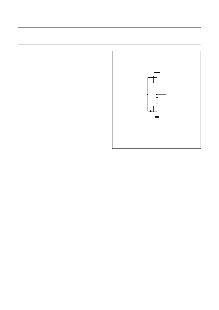
If the alarm condition is true, the voltage on pin ALARM
(see Fig.14) goes to a HIGH level (CMOS). This signal
could be used, for example, to drive pin ALS to disable the
laser driver; the signal to pin ALS has to be latched to
prevent oscillation.
A hysteresis of approximately 10% is applied to both alarm
functions. The attenuation ratios of 1:300 and 1:1500 are
valid if the bias current rises above the reference current
levels. If the bias current decreases, the ratios are 10%
lower.
Accuracy of voltage on inputs: ONE, ZERO,
ALARMLO, ALARMHI
It is important to consider the accuracy of the 1.5 V level
with respect to VCC(R) on pins ONE and ZERO if resistors
are used to set the reference currents. Although this value
is independent of VCC(R), deviations from 1.5 V can be
caused by:
Input current: At Tj =25 °C, the voltage between pin and
VCC varies from 1.58 V at an input current of 6 A, down
to 1.45 V at 65
A and 1.41 V at 100 A. The range
between 65
A and 100 A is only specified for
ALARMLO. In the application, the input current is
virtually fixed, so this variation has little effect.
Variation in batch and individual device characteristics,
not exceeding
±2% from the nominal product: This
variation can be compensated for where devices in the
application are individually trimmed.
Temperature: The variation in Tj is shown in Fig.15.
At 30
A (middle of the specified range) the total
variation in Tj is <1%, at 65 A it is <2% and at 6 Aitis
<3%.
R
ALARMHI
1.5
1500
×
I
OBIAS
() max
()
---------------------------------
=
[]
R
ALARMLO
1.5
300
×
I
O BIAS
() min
()
--------------------------------
=
[]
I
ALARMLO
610
3
–
×
300
---------------------
20
A
==
I
ALARMHI
90
10
3
–
×
1500
------------------------
60
A
==
R
ALARMHI
1.5
1500
×
90
10
3
–
×
----------------------------
25 k
==
R
ALARMLO
1.5
300
×
610
3
–
×
------------------------
75 k
==
handbook, halfpage
MGS909
20
43
VCC(R)
GND
ALARM
Fig.14 ALARM output.
相關(guān)PDF資料 |
PDF描述 |
|---|---|
| 935263881112 | SPECIALTY TELECOM CIRCUIT, PDSO28 |
| 935263881118 | SPECIALTY TELECOM CIRCUIT, PDSO28 |
| 935263971112 | SPECIALTY TELECOM CIRCUIT, PDSO28 |
| 935263971118 | SPECIALTY TELECOM CIRCUIT, PDSO28 |
| 08-040831 | OUTLINE AUTO - TANGING MEGAPAC |
相關(guān)代理商/技術(shù)參數(shù) |
參數(shù)描述 |
|---|---|
| 935264217557 | 制造商:NXP Semiconductors 功能描述:SUB ONLY IC |
| 935267356112 | 制造商:NXP Semiconductors 功能描述:IC TEA1507PN |
| 935268081112 | 制造商:NXP Semiconductors 功能描述:SUB ONLY IC |
| 935268721125 | 制造商:NXP Semiconductors 功能描述:Buffer/Line Driver 1-CH Non-Inverting 3-ST CMOS 5-Pin TSSOP T/R |
| 935269304128 | 制造商:ST-Ericsson 功能描述:IC AUDIO CODEC W/TCH SCRN 48LQFP |
發(fā)布緊急采購,3分鐘左右您將得到回復(fù)。