- 您現(xiàn)在的位置:買賣IC網(wǎng) > PDF目錄36334 > 935262922557 (NXP SEMICONDUCTORS) SPECIALTY CONSUMER CIRCUIT, PQFP160 PDF資料下載
參數(shù)資料
| 型號(hào): | 935262922557 |
| 廠商: | NXP SEMICONDUCTORS |
| 元件分類: | 消費(fèi)家電 |
| 英文描述: | SPECIALTY CONSUMER CIRCUIT, PQFP160 |
| 封裝: | PLASTIC, SOT-322, QFP-160 |
| 文件頁數(shù): | 6/147頁 |
| 文件大?。?/td> | 526K |
| 代理商: | 935262922557 |
第1頁第2頁第3頁第4頁第5頁當(dāng)前第6頁第7頁第8頁第9頁第10頁第11頁第12頁第13頁第14頁第15頁第16頁第17頁第18頁第19頁第20頁第21頁第22頁第23頁第24頁第25頁第26頁第27頁第28頁第29頁第30頁第31頁第32頁第33頁第34頁第35頁第36頁第37頁第38頁第39頁第40頁第41頁第42頁第43頁第44頁第45頁第46頁第47頁第48頁第49頁第50頁第51頁第52頁第53頁第54頁第55頁第56頁第57頁第58頁第59頁第60頁第61頁第62頁第63頁第64頁第65頁第66頁第67頁第68頁第69頁第70頁第71頁第72頁第73頁第74頁第75頁第76頁第77頁第78頁第79頁第80頁第81頁第82頁第83頁第84頁第85頁第86頁第87頁第88頁第89頁第90頁第91頁第92頁第93頁第94頁第95頁第96頁第97頁第98頁第99頁第100頁第101頁第102頁第103頁第104頁第105頁第106頁第107頁第108頁第109頁第110頁第111頁第112頁第113頁第114頁第115頁第116頁第117頁第118頁第119頁第120頁第121頁第122頁第123頁第124頁第125頁第126頁第127頁第128頁第129頁第130頁第131頁第132頁第133頁第134頁第135頁第136頁第137頁第138頁第139頁第140頁第141頁第142頁第143頁第144頁第145頁第146頁第147頁
1998 Apr 09
103
Philips Semiconductors
Product specication
Multimedia bridge, high performance
Scaler and PCI circuit (SPCI)
SAA7146A
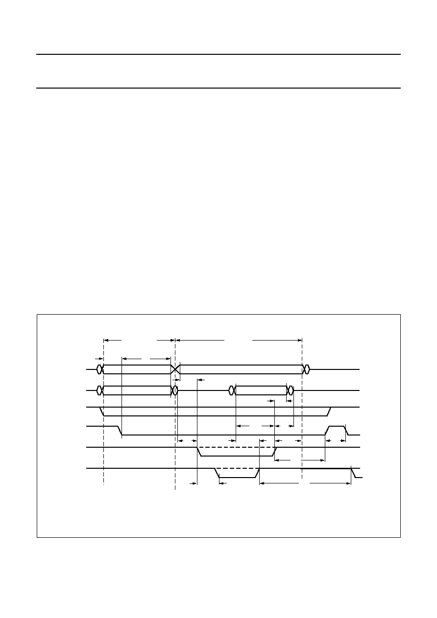
7.15.4.1
Target bus cycle in Intel mode
The SAA7146A starts a target transfer cycle by placing the
target address on the multiplexed address/data lines
(AD15 to AD0). The Address Latch Enable (ALE) is then
asserted (set LOW) indicating that the address lines
AD15 to AD0 and the SBHE signal are valid (the active
LOW SBHE indicates data transfer on the high byte lane
AD15 to AD8). After asserting ALE the AD lines are
multiplexed for data transfer. Valid data on the AD lines is
indicated by assertion of WRN in the write mode (data from
SAA7146A to target), or by assertion of RDN in the read
mode (data from target to SAA7146A). In the read mode,
it is the responsibility of the target to place data on the AD
lines as soon as possible following the assertion of RDN.
If the target does not require wait states or handshake for
data transfer, RDY should then be tied HIGH and the
TIMEOUT value should be set to 0. If the target requires
wait states, but still does not utilize handshake, then the
TIMEOUT value can be increased. The width of both WRN
and RDN pulses will be increased by 1 PCI cycle for each
count in the TIMEOUT value. If the target is capable of
handshake, to indicate when it is ready for data transfer,
then the RDY signal can be used.
Since the SAA7146A will not evaluate the RDY signal until
TIMEOUT + 1 PCI cycles have elapsed, it is
recommended that TIMEOUT be set to a minimum value
(usually 0) for maximum throughput. If the target is slow in
responding to the RDN/WRN then TIMEOUT can be
increase to allow the target time to de-assert RDY (pull to
LOW level) for the current data cycle. Once the
TIMEOUT + 1 number of PCI cycles have elapsed (from
the assertion of RDN/WRN) the transfer control is in a ‘wait
for RDY high’ state. The data transfer cycle will be ended
when a TIMEOUT condition at RDY HIGH or a rising edge
of RDY after TIMEOUT is detected. The cycle is ended by
de-asserting ALE, SBHE and RDN/WRN.
It should be noted that in the INTEL mode the timer must
be enabled (TIEN = 0). The TIMEOUT counter is used as
‘delay sampling RDY’ value to accommodate target
reaction delay in generating a valid RDY signal. TIMEOUT
is NOT used as an overall cycle watchdog timer (i.e.: to
terminate the cycle if RDY fails to become de-asserted).
The current cycle will not end and a new cycle will not start
until RDY is asserted (HIGH).
Fig.31 Intel style transfer.
handbook, full pagewidth
MHB063
address phase
tdsw
taz
tmin
address
write data
read data
data phase
tah
tas
tdhr
tdsrd
tdsrh
tdz
tidl
tdhw
talh
trdy
AD(WR)
AD(RD)
SBHE
ALE
RDN
WRN
RDY
相關(guān)PDF資料 |
PDF描述 |
|---|---|
| 935242220551 | SPECIALTY CONSUMER CIRCUIT, PQFP208 |
| 935242220557 | SPECIALTY CONSUMER CIRCUIT, PQFP208 |
| 935260698551 | SPECIALTY CONSUMER CIRCUIT, PQFP160 |
| 935260698557 | SPECIALTY CONSUMER CIRCUIT, PQFP160 |
| 935260699551 | SPECIALTY CONSUMER CIRCUIT, PQFP208 |
相關(guān)代理商/技術(shù)參數(shù) |
參數(shù)描述 |
|---|---|
| 935264217557 | 制造商:NXP Semiconductors 功能描述:SUB ONLY IC |
| 935267356112 | 制造商:NXP Semiconductors 功能描述:IC TEA1507PN |
| 935268081112 | 制造商:NXP Semiconductors 功能描述:SUB ONLY IC |
| 935268721125 | 制造商:NXP Semiconductors 功能描述:Buffer/Line Driver 1-CH Non-Inverting 3-ST CMOS 5-Pin TSSOP T/R |
| 935269304128 | 制造商:ST-Ericsson 功能描述:IC AUDIO CODEC W/TCH SCRN 48LQFP |
發(fā)布緊急采購,3分鐘左右您將得到回復(fù)。