- 您現(xiàn)在的位置:買賣IC網(wǎng) > PDF目錄24670 > 933876880602 (NXP SEMICONDUCTORS) F/FAST SERIES, ASYN NEGATIVE EDGE TRIGGERED 4-BIT UP BINARY COUNTER, PDIP14 PDF資料下載
參數(shù)資料
| 型號(hào): | 933876880602 |
| 廠商: | NXP SEMICONDUCTORS |
| 元件分類: | 計(jì)數(shù)器 |
| 英文描述: | F/FAST SERIES, ASYN NEGATIVE EDGE TRIGGERED 4-BIT UP BINARY COUNTER, PDIP14 |
| 封裝: | PLASTIC, SOT-27-1, DIP-14 |
| 文件頁(yè)數(shù): | 4/8頁(yè) |
| 文件大?。?/td> | 75K |
| 代理商: | 933876880602 |
Philips Semiconductors
Product specification
74F393
Dual 4-bit binary ripple counter
1988 Nov 01
4
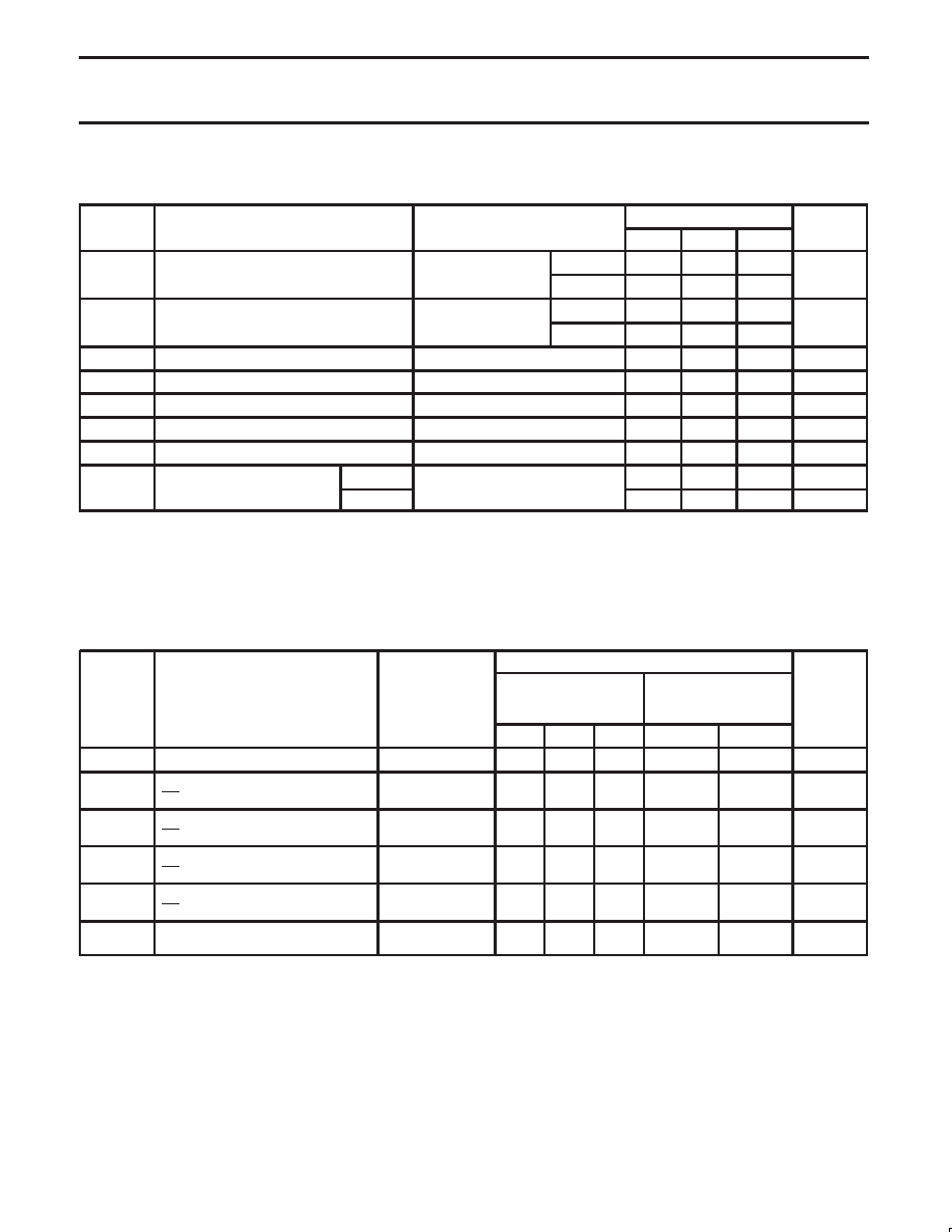
DC ELECTRICAL CHARACTERISTICS
(Over recommended operating free-air temperature range unless otherwise noted.)
SYMBOL
PARAMETER
TEST CONDITIONS1
LIMITS
UNIT
SYMBOL
PARAMETER
TEST CONDITIONS1
MIN
TYP
MAX
UNIT
VO
High level output voltage
VCC = MIN, VIL = MAX
±10%VCC
2.5
V
VOH
High-level output voltage
VIH = MIN, IOH = MAX
±5%VCC
2.7
3.4
V
VO
Low level output voltage
VCC = MIN, VIL = MAX
±10%VCC
0.30
0.50
V
VOL
Low-level output voltage
VIH = MIN, IOL = MAX
±5%VCC
0.30
0.50
V
VIK
Input clamp voltage
VCC = MIN, II = IIK
–0.73
–1.2
V
II
Input current at maximum input voltage
VCC = MAX, VI = 7.0V
100
A
IIH
High-level input current
VCC = MAX, VI = 2.7V
20
A
IIL
Low-level input current
VCC = MAX, VI = 0.5V
–0.6
mA
IOS
Short-circuit output current3
VCC = MAX
–60
–150
mA
ICC
Supply current (total)
ICCH
VCC = MAX
25
36
mA
ICC
Supply current (total)
ICCL
VCC = MAX
42
58
mA
NOTES:
1. For conditions shown as MIN or MAX, use the appropriate value specified under recommended operating conditions for the applicable type.
2. All typical values are at VCC = 5V, Tamb = 25°C.
3. Not more than one output should be shorted at a time. For testing IOS, the use of high-speed test apparatus and/or sample-and-hold
techniques are preferable in order to minimize internal heating and more accurately reflect operational values. Otherwise, prolonged shorting
of a High output may raise the chip temperature well above normal and thereby cause invalid readings in other parameter tests. In any
sequence of parameter tests, IOS tests should be performed last.
AC ELECTRICAL CHARACTERISTICS
LIMITS
SYMBOL
PARAMETER
TEST
CONDITION
VCC = +5V
Tamb = +25°C
CL = 50pF, RL = 500
VCC = +5V ± 10%
Tamb = 0°C to +70°C
CL = 50pF, RL = 500
UNIT
MIN
TYP
MAX
MIN
MAX
fMAX
Maximum clock frequency
Waveform 1
100
130
100
MHz
tPLH
tPHL
Propagation delay
CPn to Q0a or Q0b
Waveform 1
3.5
5.0
5.5
7.0
8.0
10.0
3.5
5.0
9.0
10.5
ns
tPLH
tPHL
Propagation delay
CPn to Q1a, Q1b
Waveform 1
5.0
7.5
7.0
9.5
10.0
12.0
4.5
7.0
13.0
ns
tPLH
tPHL
Propagation delay
CPn to Q2a, Q2b
Waveform 1
8.0
9.5
10.0
11.5
13.0
14.5
7.0
9.0
15.0
15.5
ns
tPLH
tPHL
Propagation delay
CPn to Q3a, Q3b
Waveform 1
10.5
12.0
12.5
14.0
15.5
16.5
10.0
11.5
17.0
17.5
ns
tPHL
Propagation delay
MR to Qna, Qnb
Waveform 2
4.0
6.0
9.0
4.0
9.0
ns
相關(guān)PDF資料 |
PDF描述 |
|---|---|
| 933906260602 | F/FAST SERIES, ASYN NEGATIVE EDGE TRIGGERED 4-BIT UP BINARY COUNTER, PDSO14 |
| 933906260623 | F/FAST SERIES, ASYN NEGATIVE EDGE TRIGGERED 4-BIT UP BINARY COUNTER, PDSO14 |
| 0561168328 | PHOSPHOR BRONZE, TIN (40) FINISH, WIRE TERMINAL |
| 933876890623 | F/FAST SERIES, OTHER DECODER/DRIVER, CONFIGURABLE OUTPUT, PDSO20 |
| 933795000602 | F/FAST SERIES, OTHER DECODER/DRIVER, CONFIGURABLE OUTPUT, PDIP20 |
相關(guān)代理商/技術(shù)參數(shù) |
參數(shù)描述 |
|---|---|
| 933879-8 | 制造商:TE Connectivity 功能描述:WHEEL, WIRE SELECTOR - Bulk |
| 933879-9 | 制造商:TE Connectivity 功能描述:WHEEL, WIRE SELECTOR - Bulk |
| 93388 | 制造商:未知廠家 制造商全稱:未知廠家 功能描述:KENNZEICHNUNG SET LABORSTECKER 4FARBEN |
| 93388 | 制造商:Multi Contact AG 功能描述:SLEEVES 6MM PLUG PK 44 |
| 933884402 | 制造商:WINTRON ELECTRONICS 功能描述: |
發(fā)布緊急采購(gòu),3分鐘左右您將得到回復(fù)。