- 您現(xiàn)在的位置:買賣IC網(wǎng) > PDF目錄24670 > 933794820602 (NXP SEMICONDUCTORS) F/FAST SERIES, SYN POSITIVE EDGE TRIGGERED 4-BIT BIDIRECTIONAL BINARY COUNTER, PDIP16 PDF資料下載
參數(shù)資料
| 型號: | 933794820602 |
| 廠商: | NXP SEMICONDUCTORS |
| 元件分類: | 計數(shù)器 |
| 英文描述: | F/FAST SERIES, SYN POSITIVE EDGE TRIGGERED 4-BIT BIDIRECTIONAL BINARY COUNTER, PDIP16 |
| 封裝: | 0.300 INCH, PLASTIC, SOT-38-4, DIP-16 |
| 文件頁數(shù): | 8/12頁 |
| 文件大小: | 104K |
| 代理商: | 933794820602 |
Philips Semiconductors
Product specification
74F193
Up/down binary counter with separate up/down clocks
1995 Jul 17
5
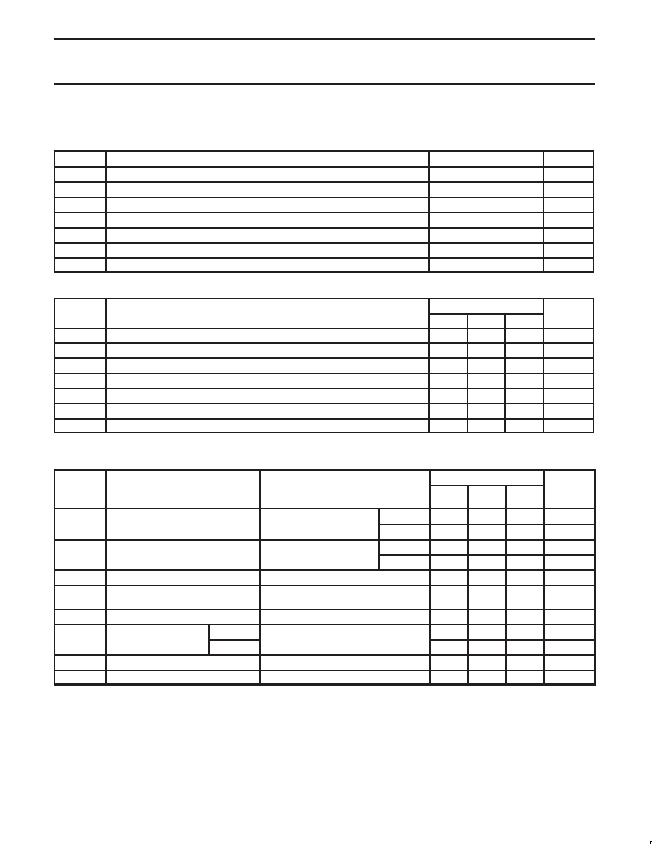
ABSOLUTE MAXIMUM RATINGS
(Operation beyond the limits set forth in this table may impair the useful life of the device. Unless otherwise noted these limits are over the
operating free-air temperature range.)
SYMBOL
PARAMETER
RATING
UNIT
VCC
Supply voltage
–0.5 to +7.0
V
VIN
Input voltage
–0.5 to +7.0
V
IIN
Input current
–30 to +5.0
mA
VOUT
Voltage applied to output in High output state
–0.5 to +VCC
V
IOUT
Current applied to output in Low output state
40
mA
Tamb
Operating free-air temperature range
0 to +70
°C
Tstg
Storage temperature
–65 to +150
°C
RECOMMENDED OPERATING CONDITIONS
SYMBOL
PARAMETER
LIMITS
UNIT
SYMBOL
PARAMETER
MIN
NOM
MAX
UNIT
VCC
Supply voltage
4.5
5.0
5.5
V
VIH
High-level input voltage
2.0
V
VIL
Low-level input voltage
0.8
V
IIK
Input clamp current
–18
mA
IOH
High-level output current
–1
mA
IOL
Low-level output current
20
mA
Tamb
Operating free-air temperature range
0
+70
°C
DC ELECTRICAL CHARACTERISTICS
(Over recommended operating free-air temperature range unless otherwise noted.)
NO TAG
LIMITS
SYMBOL
PARAMETER
TEST CONDITIONSNO TAG
MIN
TYP
NO TAG
MAX
UNIT
VO
High level output voltage
VCC = MIN, VIL = MAX,
"10%VCC
2.5
V
VOH
High-level output voltage
VCC = MIN, VIL = MAX,
IOH = MAX, VIH = MIN
"5%VCC
2.7
3.4
V
VO
Low level output voltage
VCC = MIN, VIL = MAX,
"10%VCC
0.35
0.50
V
VOL
Low-level output voltage
VCC = MIN, VIL = MAX,
IOL = MAX, VIH = MIN
"5%VCC
0.35
0.50
V
VIK
Input clamp voltage
VCC = MIN, II = IIK
–0.73
–1.2
V
II
Input current at maximum
input voltage
VCC = MAX, VI = 7.0V
100
A
IIH
High-level input current
VCC = MAX, VI = 2.7V
20
A
IIL
Low-level input
CPU, CPD
VCC = MAX V =0 5V
–1.8
mA
Low level in ut
current
Others
VCC = MAX, VI = 0.5V
–0.6
mA
IOS
Short-circuit output currentNO TAG
VCC = MAX
–60
–150
mA
ICC
Supply current (total)4
VCC = MAX
32
50
mA
NOTES:
1. For conditions shown as MIN or MAX, use the appropriate value specified under recommended operating conditions for the applicable type.
2. All typical values are at VCC = 5V, Tamb = 25°C.
3. Not more than one output should be shorted at a time. For testing IOS, the use of high-speed test apparatus and/or sample-and-hold
techniques are preferable in order to minimize internal heating and more accurately reflect operational values. Otherwise, prolonged shorting
of a High output may raise the chip temperature well above normal and thereby cause invalid readings in other parameter tests. In any
sequence of parameter tests, IOS tests should be performed last.
4. Measure ICC with parallel load and Master reset inputs grounded, all other inputs at 4.5V and all outputs open.
相關(guān)PDF資料 |
PDF描述 |
|---|---|
| 933890190112 | 800 mA, 55 V, NPN, Si, SMALL SIGNAL TRANSISTOR, TO-92 |
| 933890190126 | 800 mA, 55 V, NPN, Si, SMALL SIGNAL TRANSISTOR, TO-92 |
| 0561188328 | PHOSPHOR BRONZE, TIN (40) FINISH, WIRE TERMINAL |
| 933890540115 | 600 mA, 40 V, NPN, Si, SMALL SIGNAL TRANSISTOR |
| 933890550115 | 600 mA, 40 V, PNP, Si, SMALL SIGNAL TRANSISTOR |
相關(guān)代理商/技術(shù)參數(shù) |
參數(shù)描述 |
|---|---|
| 9337-A17R | 制造商:GC Electronics 功能描述: |
| 9337C | 制造商:Hubbell Premise Wiring 功能描述: |
| 9337-CHR-100 | 制造商:Belden Inc 功能描述: |
| 9337CKE100M | 制造商:RFMD 制造商全稱:RF Micro Devices 功能描述:380W GaN WIDEBAND PULSED |
| 9337CMG | 制造商:Apex Tool Group 功能描述:7 IN. DIAGONAL CUTTING S J PLIERS W/CO-MOLDED GRIPS, LASER HARDENED EDGES, CDD |
發(fā)布緊急采購,3分鐘左右您將得到回復(fù)。