- 您現(xiàn)在的位置:買(mǎi)賣(mài)IC網(wǎng) > PDF目錄36320 > 933768140118 (NXP SEMICONDUCTORS) SPECIALTY ANALOG CIRCUIT, PDSO16 PDF資料下載
參數(shù)資料
| 型號(hào): | 933768140118 |
| 廠商: | NXP SEMICONDUCTORS |
| 元件分類(lèi): | 模擬信號(hào)調(diào)理 |
| 英文描述: | SPECIALTY ANALOG CIRCUIT, PDSO16 |
| 封裝: | 7.50 MM, PLASTIC, MS-013, SOT-162-1, SO-16 |
| 文件頁(yè)數(shù): | 28/28頁(yè) |
| 文件大小: | 139K |
| 代理商: | 933768140118 |
第1頁(yè)第2頁(yè)第3頁(yè)第4頁(yè)第5頁(yè)第6頁(yè)第7頁(yè)第8頁(yè)第9頁(yè)第10頁(yè)第11頁(yè)第12頁(yè)第13頁(yè)第14頁(yè)第15頁(yè)第16頁(yè)第17頁(yè)第18頁(yè)第19頁(yè)第20頁(yè)第21頁(yè)第22頁(yè)第23頁(yè)第24頁(yè)第25頁(yè)第26頁(yè)第27頁(yè)當(dāng)前第28頁(yè)
2003 Jan 27
9
Philips Semiconductors
Product specication
8-bit A/D and D/A converter
PCF8591
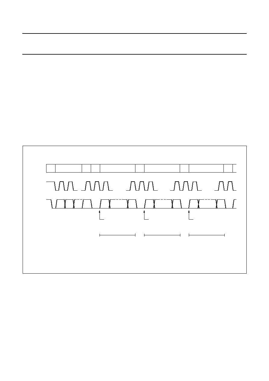
7.4
A/D conversion
The A/D converter makes use of the successive
approximation conversion technique. The on-chip D/A
converter and a high-gain comparator are used
temporarily during an A/D conversion cycle.
An A/D conversion cycle is always started after sending a
valid read mode address to a PCF8591 device. The A/D
conversion cycle is triggered at the trailing edge of the
acknowledge clock pulse and is executed while
transmitting the result of the previous conversion (see
Fig.9).
Once a conversion cycle is triggered an input voltage
sample of the selected channel is stored on the chip and is
converted to the corresponding 8-bit binary code. Samples
picked up from differential inputs are converted to an 8-bit
twos complement code (see Figs 10 and 11).
The conversion result is stored in the ADC data register
and awaits transmission. If the auto-increment flag is set
the next channel is selected.
The first byte transmitted in a read cycle contains the
conversion result code of the previous read cycle. After a
Power-on reset condition the first byte read is a
hexadecimal 80. The protocol of an I2C-bus read cycle is
shown in Chapter 8, Figs 16 and 17.
The maximum A/D conversion rate is given by the actual
speed of the I2C-bus.
handbook, full pagewidth
S
1
A
ADDRESS
DATA BYTE 1
DATA BYTE 2
DATA BYTE 0
12
9
81
91
PROTOCOL
SCL
SDA
conversion of byte 2
conversion of byte 3
conversion of byte 1
transmission
of previously
converted byte
sampling byte 2
sampling byte 3
sampling byte 1
transmission
of byte 1
transmission
of byte 2
MBL829
Fig.9 A/D conversion sequence.
相關(guān)PDF資料 |
PDF描述 |
|---|---|
| 933768140112 | SPECIALTY ANALOG CIRCUIT, PDSO16 |
| 933772-023 | SIMPLEX SMA CONNECTOR |
| 936045-007 | SIMPLEX SMA CONNECTOR |
| 936047-013 | SIMPLEX SMA CONNECTOR |
| 936047-018 | SIMPLEX SMA CONNECTOR |
相關(guān)代理商/技術(shù)參數(shù) |
參數(shù)描述 |
|---|---|
| 93378-003 | 制造商:FCI 功能描述:MEMORY CARD RECEPTACLE - Bulk |
| 9337-A17R | 制造商:GC Electronics 功能描述: |
| 9337C | 制造商:Hubbell Premise Wiring 功能描述: |
| 9337-CHR-100 | 制造商:Belden Inc 功能描述: |
| 9337CKE100M | 制造商:RFMD 制造商全稱(chēng):RF Micro Devices 功能描述:380W GaN WIDEBAND PULSED |
發(fā)布緊急采購(gòu),3分鐘左右您將得到回復(fù)。