- 您現(xiàn)在的位置:買賣IC網(wǎng) > PDF目錄36320 > 933768140118 (NXP SEMICONDUCTORS) SPECIALTY ANALOG CIRCUIT, PDSO16 PDF資料下載
參數(shù)資料
| 型號(hào): | 933768140118 |
| 廠商: | NXP SEMICONDUCTORS |
| 元件分類: | 模擬信號(hào)調(diào)理 |
| 英文描述: | SPECIALTY ANALOG CIRCUIT, PDSO16 |
| 封裝: | 7.50 MM, PLASTIC, MS-013, SOT-162-1, SO-16 |
| 文件頁(yè)數(shù): | 24/28頁(yè) |
| 文件大?。?/td> | 139K |
| 代理商: | 933768140118 |
第1頁(yè)第2頁(yè)第3頁(yè)第4頁(yè)第5頁(yè)第6頁(yè)第7頁(yè)第8頁(yè)第9頁(yè)第10頁(yè)第11頁(yè)第12頁(yè)第13頁(yè)第14頁(yè)第15頁(yè)第16頁(yè)第17頁(yè)第18頁(yè)第19頁(yè)第20頁(yè)第21頁(yè)第22頁(yè)第23頁(yè)當(dāng)前第24頁(yè)第25頁(yè)第26頁(yè)第27頁(yè)第28頁(yè)
2003 Jan 27
5
Philips Semiconductors
Product specication
8-bit A/D and D/A converter
PCF8591
7
FUNCTIONAL DESCRIPTION
7.1
Addressing
Each PCF8591 device in an I2C-bus system is activated by
sending a valid address to the device. The address
consists of a fixed part and a programmable part. The
programmable part must be set according to the address
pins A0, A1 and A2. The address always has to be sent as
the first byte after the start condition in the I2C-bus
protocol. The last bit of the address byte is the
read/write-bit which sets the direction of the following data
transfer (see Figs 4, 16 and 17).
7.2
Control byte
The second byte sent to a PCF8591 device will be stored
in its control register and is required to control the device
function. The upper nibble of the control register is used for
enabling the analog output, and for programming the
analog inputs as single-ended or differential inputs. The
lower nibble selects one of the analog input channels
defined by the upper nibble (see Fig.5). If the
auto-increment flag is set, the channel number is
incremented automatically after each A/D conversion.
If the auto-increment mode is desired in applications
where the internal oscillator is used, the analog output
enable flag in the control byte (bit 6) should be set. This
allows the internal oscillator to run continuously, thereby
preventing conversion errors resulting from oscillator
start-up delay. The analog output enable flag may be reset
at other times to reduce quiescent power consumption.
The selection of a non-existing input channel results in the
highest available channel number being allocated.
Therefore, if the auto-increment flag is set, the next
selected channel will be always channel 0. The most
significant bits of both nibbles are reserved for future
functions and have to be set to logic 0. After a Power-on
reset condition all bits of the control register are reset to
logic 0. The D/A converter and the oscillator are disabled
for power saving. The analog output is switched to a
high-impedance state.
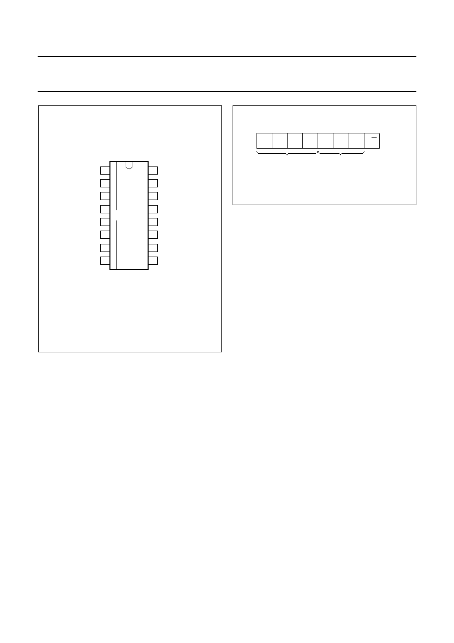
handbook, halfpage
MBL823
1
2
3
4
5
6
7
8
16
15
14
13
12
11
10
9
AIN0
AIN1
AIN2
AIN3
A0
A1
A2
VSS
VDD
AOUT
VREF
AGND
EXT
OSC
SCL
SDA
PCF8591T
Fig.3 Pinning diagram (SO16).
handbook, halfpage
MBL824
1
msb
lsb
0
fixed part
programmable part
1
A2
A1
A0
R/W
Fig.4 Address byte.
相關(guān)PDF資料 |
PDF描述 |
|---|---|
| 933768140112 | SPECIALTY ANALOG CIRCUIT, PDSO16 |
| 933772-023 | SIMPLEX SMA CONNECTOR |
| 936045-007 | SIMPLEX SMA CONNECTOR |
| 936047-013 | SIMPLEX SMA CONNECTOR |
| 936047-018 | SIMPLEX SMA CONNECTOR |
相關(guān)代理商/技術(shù)參數(shù) |
參數(shù)描述 |
|---|---|
| 93378-003 | 制造商:FCI 功能描述:MEMORY CARD RECEPTACLE - Bulk |
| 9337-A17R | 制造商:GC Electronics 功能描述: |
| 9337C | 制造商:Hubbell Premise Wiring 功能描述: |
| 9337-CHR-100 | 制造商:Belden Inc 功能描述: |
| 9337CKE100M | 制造商:RFMD 制造商全稱:RF Micro Devices 功能描述:380W GaN WIDEBAND PULSED |
發(fā)布緊急采購(gòu),3分鐘左右您將得到回復(fù)。