- 您現(xiàn)在的位置:買賣IC網(wǎng) > PDF目錄369352 > 795T (意法半導(dǎo)體) 3V Supervisor with Battery Switchover PDF資料下載
參數(shù)資料
| 型號: | 795T |
| 廠商: | 意法半導(dǎo)體 |
| 英文描述: | 3V Supervisor with Battery Switchover |
| 中文描述: | 3V的監(jiān)控與電池切換 |
| 文件頁數(shù): | 10/32頁 |
| 文件大小: | 304K |
| 代理商: | 795T |
第1頁第2頁第3頁第4頁第5頁第6頁第7頁第8頁第9頁當(dāng)前第10頁第11頁第12頁第13頁第14頁第15頁第16頁第17頁第18頁第19頁第20頁第21頁第22頁第23頁第24頁第25頁第26頁第27頁第28頁第29頁第30頁第31頁第32頁

STM690/704/795/802/804/805/806
10/32
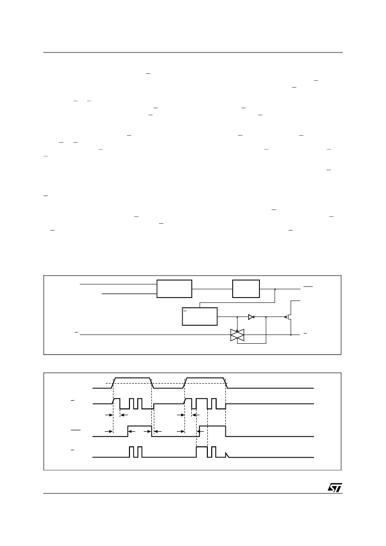
Chip-Enable Gating (STM795 only)
Internal gating of the chip enable (E) signal pre-
vents erroneous data from corrupting the external
CMOS RAM in the event of an undervoltage con-
dition. The STM795 uses a series transmission
gate from E to E
CON
(see Figure
12
). During nor-
mal operation (reset not asserted), the E transmis-
sion gate is enabled and passes all E transitions.
When reset is asserted, this path becomes dis-
abled, preventing erroneous data from corrupting
the CMOS RAM. The short E propagation delay
from E to E
CON
enables the STM795 to be used
with most μPs. If E is low when reset asserts,
E
CON
remains low for typically 10μs to permit the
current WRITE cycle to complete.
Chip Enable Input (STM795 only)
The chip-enable transmission gate is disabled and
E is high impedance (disabled mode) while reset
is asserted. During a power-down sequence when
V
CC
passes the reset threshold, the chip-enable
transmission gate disables and E immediately be-
comes high impedance if the voltage at E is high.
If E is low when reset asserts, the chip-enable
transmission gate will disable 10μs after reset as-
serts (see Figure
13
). This permits the current
WRITE cycle to complete during power-down.
Any time a reset is generated, the chip-enable
transmission gate remains disabled and E remains
high impedance (regardless of E activity) for the
first half of the reset time-out period (t
rec
/2). When
the chip enable transmission gate is enabled, the
impedance of E appears as a 40
resistor in se-
ries with the load at E
CON
. The propagation delay
through the chip-enable transmission gate de-
pends on V
CC
, the source impedance of the drive
connected to E, and the loading on E
CON
. The chip
enable propagation delay is production tested
from the 50% point on E to the 50% point on E
CON
using a 50
driver and a 50pF load capacitance
(see
Figure 36., page 23
). For minimum propaga-
tion delay, minimize the capacitive load at E
CON
and use a low-output impedance driver.
Chip Enable Output (STM795 only)
When the chip-enable transmission gate is en-
abled, the impedance of E
CON
is equivalent to a
40
resistor in series with the source driving E. In
the disabled mode, the transmission gate is off
and an active pull-up connects E
CON
to V
OUT
(see
Figure
12
). This pull-up turns off when the trans-
mission gate is enabled.
Figure 12. Chip-Enable Gating
Figure 13. Chip Enable Waveform (STM795)
AI08802
V
RST
V
OUT
V
CC
COMPARE
E
CON
t
Generator
E
CON
OUTPUT
CONTROL
RST
E
AI08855c
RST
E
V
CC
V
RST
V
BAT
E
CON
trec
trec
trec
trec
10μs
相關(guān)PDF資料 |
PDF描述 |
|---|---|
| 79600A | Three-Terminal Low Current Negative Voltage Regulators |
| 79L08AC | Three-Terminal Low Current Negative Voltage Regulators |
| 79L08ACD | Three-Terminal Low Current Negative Voltage Regulators |
| 79L08ACF | Three-Terminal Low Current Negative Voltage Regulators |
| 79L08ACZ | Three-Terminal Low Current Negative Voltage Regulators |
相關(guān)代理商/技術(shù)參數(shù) |
參數(shù)描述 |
|---|---|
| 795XFL-2 CAL | 制造商:Starrett Company 功能描述:CALIBRATED - 1-2" 25-50MM ELECTRONIC MICROMETER WITH OUTPUT |
| 795XFL-2 CAL DU | 制造商:Starrett Company 功能描述:CALIBRATED W/ DATA & UNCERTAINTIES - 1-2" 25-50MM ELECTRONIC MICROMETER WITH OUT |
| 796 | 功能描述:電路板硬件 - PCB NYL Rd Clr Hle Spcr 1.00 .312OD #10 RoHS:否 制造商:Harwin 類型:Shield Clip 長度:9.4 mm 螺紋大小: 外徑: 材料:Beryllium Copper 電鍍:Tin |
| 79600 | 制造商:Amphenol 功能描述:AMPHENOL TNC JACK S9B2B 制造商:TE Connectivity 功能描述: |
| 796-002ZNUA-18 | 制造商:Glenair Inc 功能描述:MILITARY ACCESSORIES - Bulk |
發(fā)布緊急采購,3分鐘左右您將得到回復(fù)。