- 您現(xiàn)在的位置:買賣IC網(wǎng) > PDF目錄360502 > 74LVT00PWDH (NXP SEMICONDUCTORS) 3.3V Quad 2-input NAND gate PDF資料下載
參數(shù)資料
| 型號: | 74LVT00PWDH |
| 廠商: | NXP SEMICONDUCTORS |
| 元件分類: | 通用總線功能 |
| 英文描述: | 3.3V Quad 2-input NAND gate |
| 中文描述: | LVT SERIES, QUAD 2-INPUT NAND GATE, PDSO14 |
| 封裝: | PLASTIC, SOT-402, TSSOP-14 |
| 文件頁數(shù): | 3/10頁 |
| 文件大?。?/td> | 81K |
| 代理商: | 74LVT00PWDH |
Philips Semiconductors
Product specification
74LVT00
3.3V Quad 2-input NAND gate
1996 Aug 15
3
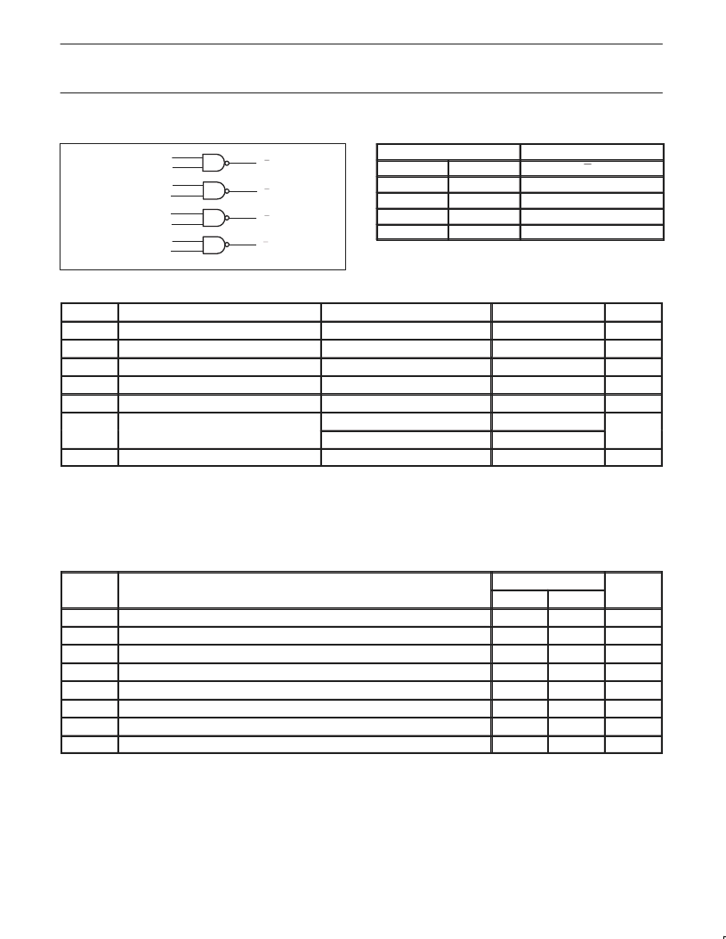
LOGIC DIAGRAM
A0
B0
A1
B1
A2
B2
Y0
A3
B3
Y1
Y2
Y3
V
= Pin 14
GND = Pin 7
3
6
8
11
1
2
4
5
9
10
12
13
SA00360
FUNCTION TABLE
INPUTS
OUTPUT
Dna
Dnb
Qn
L
L
H
L
H
H
H
L
H
H
H
L
NOTES:
H = High voltage level
L
= Low voltage level
ABSOLUTE MAXIMUM RATINGS
1, 2
SYMBOL
PARAMETER
CONDITIONS
RATING
UNIT
V
CC
DC supply voltage
–0.5 to +4.6
V
I
IK
DC input diode current
V
I
< 0
–50
mA
V
I
DC input voltage
3
–0.5 to +7.0
V
I
OK
DC output diode current
V
O
< 0
–50
mA
V
OUT
DC output voltage
3
Output in Off or High state
–0.5 to +7.0
V
I
OUT
DC output current
Output in High state
–32
mA
Output in Low state
64
T
stg
Storage temperature range
–65 to 150
°
C
NOTES:
1. Stresses beyond those listed may cause permanent damage to the device. These are stress ratings only and functional operation of the
device at these or any other conditions beyond those indicated under “recommended operating conditions” is not implied. Exposure to
absolute-maximum-rated conditions for extended periods may affect device reliability.
2. The performance capability of a high-performance integrated circuit in conjunction with its thermal environment can create junction
temperatures which are detrimental to reliability. The maximum junction temperature of this integrated circuit should not exceed 150
°
C.
3. The input and output negative voltage ratings may be exceeded if the input and output clamp current ratings are observed.
RECOMMENDED OPERATING CONDITIONS
SYMBOL
PARAMETER
LIMITS
UNIT
MIN
MAX
V
CC
DC supply voltage
2.7
3.6
V
V
I
Input voltage
0
5.5
V
V
IH
High-level input voltage
2.0
V
V
IL
Low-level Input voltage
0.8
V
I
OH
High-level output current
–20
mA
I
OL
Low-level output current
32
mA
t/
v
Input transition rise or fall rate; Outputs enabled
10
ns/V
T
amb
Operating free-air temperature range
–40
+85
°
C
相關(guān)PDF資料 |
PDF描述 |
|---|---|
| 74LVT02 | 3.3V Quad 2-input NOR gate |
| 74LVT02PWDH | 3.3V Quad 2-input NOR gate |
| 74LVT04 | 3.3V Hex inverter |
| 74LVT04PWDH | 3.3V Hex inverter |
| 74LVT08PWDH | 3.3V Quad 2-input AND gate |
相關(guān)代理商/技術(shù)參數(shù) |
參數(shù)描述 |
|---|---|
| 74LVT00PW-T | 功能描述:邏輯門 3.3V QUAD 2-INPUT NAND GATE RoHS:否 制造商:Texas Instruments 產(chǎn)品:OR 邏輯系列:LVC 柵極數(shù)量:2 線路數(shù)量(輸入/輸出):2 / 1 高電平輸出電流:- 16 mA 低電平輸出電流:16 mA 傳播延遲時間:3.8 ns 電源電壓-最大:5.5 V 電源電壓-最小:1.65 V 最大工作溫度:+ 125 C 安裝風格:SMD/SMT 封裝 / 箱體:DCU-8 封裝:Reel |
| 74LVT02D | 功能描述:邏輯門 3.3V QUAD 2-INPUT NOR GATE RoHS:否 制造商:Texas Instruments 產(chǎn)品:OR 邏輯系列:LVC 柵極數(shù)量:2 線路數(shù)量(輸入/輸出):2 / 1 高電平輸出電流:- 16 mA 低電平輸出電流:16 mA 傳播延遲時間:3.8 ns 電源電壓-最大:5.5 V 電源電壓-最小:1.65 V 最大工作溫度:+ 125 C 安裝風格:SMD/SMT 封裝 / 箱體:DCU-8 封裝:Reel |
| 74LVT02D,112 | 功能描述:邏輯門 3.3V QUAD 2-INPUT RoHS:否 制造商:Texas Instruments 產(chǎn)品:OR 邏輯系列:LVC 柵極數(shù)量:2 線路數(shù)量(輸入/輸出):2 / 1 高電平輸出電流:- 16 mA 低電平輸出電流:16 mA 傳播延遲時間:3.8 ns 電源電壓-最大:5.5 V 電源電壓-最小:1.65 V 最大工作溫度:+ 125 C 安裝風格:SMD/SMT 封裝 / 箱體:DCU-8 封裝:Reel |
| 74LVT02D,118 | 功能描述:邏輯門 3.3V QUAD 2-INPUT RoHS:否 制造商:Texas Instruments 產(chǎn)品:OR 邏輯系列:LVC 柵極數(shù)量:2 線路數(shù)量(輸入/輸出):2 / 1 高電平輸出電流:- 16 mA 低電平輸出電流:16 mA 傳播延遲時間:3.8 ns 電源電壓-最大:5.5 V 電源電壓-最小:1.65 V 最大工作溫度:+ 125 C 安裝風格:SMD/SMT 封裝 / 箱體:DCU-8 封裝:Reel |
| 74LVT02DB | 功能描述:邏輯門 3.3V QUAD 2-INPUT NOR GATE RoHS:否 制造商:Texas Instruments 產(chǎn)品:OR 邏輯系列:LVC 柵極數(shù)量:2 線路數(shù)量(輸入/輸出):2 / 1 高電平輸出電流:- 16 mA 低電平輸出電流:16 mA 傳播延遲時間:3.8 ns 電源電壓-最大:5.5 V 電源電壓-最小:1.65 V 最大工作溫度:+ 125 C 安裝風格:SMD/SMT 封裝 / 箱體:DCU-8 封裝:Reel |
發(fā)布緊急采購,3分鐘左右您將得到回復。