- 您現(xiàn)在的位置:買賣IC網(wǎng) > PDF目錄360443 > 74F723A (NXP Semiconductors N.V.) CONN DSUB PLUG 15POS VERT PCB PDF資料下載
參數(shù)資料
| 型號(hào): | 74F723A |
| 廠商: | NXP Semiconductors N.V. |
| 英文描述: | CONN DSUB PLUG 15POS VERT PCB |
| 中文描述: | 四2選1數(shù)據(jù)選擇器多路三態(tài) |
| 文件頁(yè)數(shù): | 2/14頁(yè) |
| 文件大小: | 104K |
| 代理商: | 74F723A |
第1頁(yè)當(dāng)前第2頁(yè)第3頁(yè)第4頁(yè)第5頁(yè)第6頁(yè)第7頁(yè)第8頁(yè)第9頁(yè)第10頁(yè)第11頁(yè)第12頁(yè)第13頁(yè)第14頁(yè)
Philips Semiconductors
Product specification
74F723A/74F723–1/
74F725A/74F725–1
Multiplexers
74F723A Quad 3-to-1 Data Selector Multiplexer (3-State)
74F723-1 Quad 3-to-1 Data Selector Multiplexer with 30 Equivalent Output Termination Impedance (3-State)
74F725A Quad 4-to-1 Data Selector Multiplexer
74F725-1 Quad 4-to-1 Data Selector Multiplexer with 30 Equivalent Output Termination Impedance
2
1990 Dec 13
853-1369 01257
FEATURES for 74F723A/74F723-1
Consists of four 3-to-1 Multiplexers
High impedance PNP base inputs for reduced loading
(20
μ
A in High and Low states)
Inverting or non-inverting data path capability by an inverting (INV)
input
Designed for address multiplexing of dynamic RAM and other
applications
Multiple side pins for V
CC
and GND to reduce lead inductance
(improves speed and noise immunity)
3-State outputs sink 64mA (74F723A only)
30 termination impedance on each output – 74F723-1
FEATURES for 74F725A/74F725-1
Consists of four 4-to-1 Multiplexers
High impedance PNP base inputs for reduced loading
(20
μ
A in High and Low states)
Equivalent to two 74F253s without 3-State
Outputs sink 64mA (74F725A only)
30 termination impedance on each output – 74F725-1
DESCRIPTION
The 74F723A/74F723-1 consist of four 3-to-1 multiplexers designed
for address multiplexing of dynamic RAMs and other multiplexing
applications. Select (S0, S1) inputs control which line is to be
selected, as defined in the Function Table for 74F723A/74F723-1.
When the invering input (INV) is Low, the input data path is inverted.
To improve speed and noise immunity, V
CC
and GND side pins are
used. The 3-State outputs source 15mA and sink 64mA. The
74F723-1 is the same as 74F723A except that it has a 30
temination impedance on each output to reduce line noise and the
3-State outputs sink 5mA.
The 74F725A/74F725-1 consist of four 4-to1 multiplexers designed
for general multiplexing purpose. The select (S0, S1) inputs control
which line is to be selected, as defined in the Function Table for
74F725A/725-1. The outputs source 15mA and sink 64mA. The
74F725-1 is the same as the 74F725A except that it has a 30
termination impedance on each output to reduce line noise and the
outputs sink 5mA.
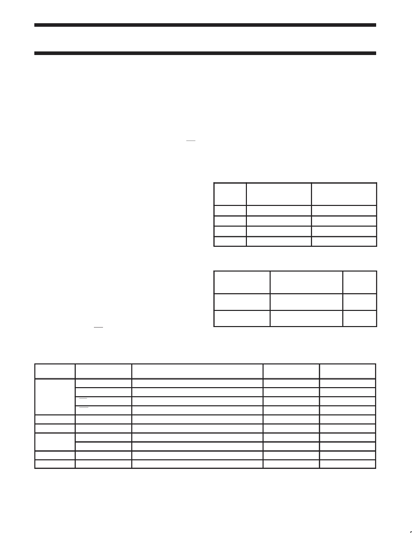
TYPE
TYPICAL
PROPAGATION DELAY
TYPICAL SUPPLY
CURRENT
(TOTAL)
74F723A
5.5ns
25mA
74F723-1
7.0ns
26mA
74F725A
5.5ns
20mA
74F725-1
6.5ns
20mA
ORDERING INFORMATION
DESCRIPTION
COMMERCIAL RANGE
V
CC
= 5V
±
10%
T
amb
= 0
°
C to +70
°
C
PKG DWG
#
20-Pin Plastic Slim
DIP (300 mil)
N74F723AN, N74F723-1N,
N74F725AN, N74F725-1N
SOT222 1
SOT222-1
,
24 Pin Plastic SOL
24-Pin Plastic SOL
N74F723AD, N74F723-1D,
N74F725AD, N74F725-1D
SOT137 1
SOT137-1
,
INPUT AND OUTPUT LOADING AND FAN-OUT TABLE
TYPE
PINS
DESCRIPTION
74F(U.L.)
HIGH/LOW
1.0/0.066
LOAD VALUE
HIGH/LOW
20
μ
A/40
μ
A
20
μ
A/20
μ
A
20
μ
A/20
μ
A
20
μ
A/20
μ
A
15mA/64mA
15mA/5mA
20
μ
A/40
μ
A
20
μ
A/20
μ
A
15mA/64mA
15mA/5mA
Dna, Dnb, Dnc
Data inputs
74F723A/
74F723-1
S0, S1
Select inputs
1.0/0.033
OE
Output Enable input
1.0/0.033
INV
Q0 - Q3
Q0 - Q3
Output inverting input
Data outputs for 74F723A
Data outputs for 74F723-1
1.0/0.033
750/106.7
750/8.33
74F723A
74F723-1
74F725A/
74F725-1
Dna, Dnb, Dnc, Dnd
Data inputs
1.0/0.066
S0, S1
Q0 - Q3
Q0 - Q3
Select inputs
Data outputs
Data outputs
1.0/0.033
750/106.7
750/8.33
74F725A
74F725-1
NOTE:
One (1.0) FAST Unit Load (U.L.) is defined as: 20
μ
A in the High state and 0.6mA in the Low state.
相關(guān)PDF資料 |
PDF描述 |
|---|---|
| 74F725-1 | Quad 2-to-1 data selector multiplexer 3-State |
| 74F725A | Quad 2-to-1 data selector multiplexer 3-State |
| 74F723A74F723-174F725A74F725-1 | Quad 2-to-1 data selector multiplexer (3-State) |
| 74F74 | Dual D-type flip-flop |
| 74F74DC | Dual D-Type Flip-Flop |
相關(guān)代理商/技術(shù)參數(shù) |
參數(shù)描述 |
|---|---|
| 74F723A74F723-174F725A74F725-1 | 制造商:未知廠家 制造商全稱:未知廠家 功能描述:Quad 2-to-1 data selector multiplexer (3-State) |
| 74F724PC | 制造商:Rochester Electronics LLC 功能描述:- Bulk |
| 74F725-1 | 制造商:PHILIPS 制造商全稱:NXP Semiconductors 功能描述:Quad 2-to-1 data selector multiplexer 3-State |
| 74F725A | 制造商:PHILIPS 制造商全稱:NXP Semiconductors 功能描述:Quad 2-to-1 data selector multiplexer 3-State |
| 74F74 | 制造商:NSC 制造商全稱:National Semiconductor 功能描述:Dual D-Type Positive Edge-Triggered Flip-Flop |
發(fā)布緊急采購(gòu),3分鐘左右您將得到回復(fù)。