- 您現在的位置:買賣IC網 > PDF目錄375057 > 74ABT16244 (Fairchild Semiconductor Corporation) 16-Bit Buffer/Line Driver with 3-STATE Outputs PDF資料下載
參數資料
| 型號: | 74ABT16244 |
| 廠商: | Fairchild Semiconductor Corporation |
| 英文描述: | 16-Bit Buffer/Line Driver with 3-STATE Outputs |
| 中文描述: | 16位緩沖器/線路驅動器3態(tài)輸出 |
| 文件頁數: | 4/8頁 |
| 文件大?。?/td> | 100K |
| 代理商: | 74ABT16244 |
www.fairchildsemi.com
4
7
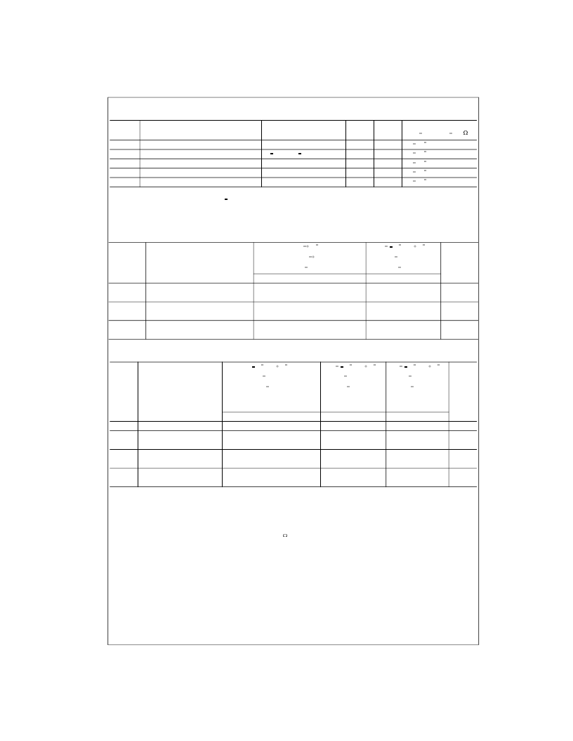
DC Electrical Characteristics
Note 4:
Max number of outputs defined as (n). n-1 data inputs are driven 0V to 3V. One output at LOW. Guaranteed, but not tested.
Note 5:
Max number of outputs defined as (n). n 1 data inputs are driven 0V to 3V. One output HIGH. Guaranteed, but not tested.
Note 6:
Max number of data inputs (n) switching. n-1 inputs switching 0V to 3V. Input-under-test switching: 3V to threshold (V
ILD
), 0V to threshold (V
IHD
).
Guaranteed, but not tested.
AC Electrical Characteristics
Extended AC Electrical Characteristics
Note 7:
This specification is guaranteed but not tested. The limits apply to propagation delays for all paths described switching in phase
(i.e., all LOW-to-HIGH, HIGH-to-LOW, etc.).
Note 8:
This specification is guaranteed but not tested. The limits represent propagation delay with 250 pF load capacitors in place of the 50 pF load
capacitors in the standard AC load. This specification pertains to single output switching only.
Note 9:
This specification is guaranteed but not tested. The limits represent propagation delays for all paths described switching in phase
(i.e., all LOW-to-HIGH, HIGH-to-LOW, etc.) with 250 pF load capacitors in place of the 50 pF load capacitors in the standard AC load.
Note 10:
The 3-STATE delay times are dominated by the RC network (500
:
, 250 pF) on the output and have been excluded from the datasheet.
Symbol
Parameter
Min
Typ
Max
Units
V
CC
Conditions
C
L
50 pF, R
L
500
:
T
A
25
q
C (Note 4)
T
A
25
q
C (Note 4)
T
A
25
q
C (Note 5)
T
A
25
q
C (Note 6)
T
A
25
q
C (Note 6)
V
OLP
V
OLV
V
OHV
V
IHD
V
ILD
Quiet Output Maximum Dynamic V
OL
Quiet Output Minimum Dynamic V
OL
Minimum HIGH Level Dynamic Output Voltage
0.4
1.0
3.0
0.7
V
V
V
5.0
5.0
5.0
1.3
2.7
Minimum HIGH Level Dynamic Input Voltage
Maximum LOW Level Dynamic Input Voltage
2.0
1.4
1.2
V
V
5.0
5.0
0.8
Symbol
Parameter
T
A
25
q
C
V
CC
5V
C
L
50 pF
Typ
2.3
2.7
T
A
40
q
C to 85
q
C
V
CC
4.5V
–
5.5V
C
L
50 pF
Min
1.0
1.0
Units
Min
1.0
1.0
Max
3.9
3.9
Max
3.9
3.9
t
PLH
t
PHL
t
PZH
t
PZL
t
PHZ
t
PLZ
Propagation
Delay Data to Outputs
ns
Output Enable
Time
Output Disable
1.5
1.5
1.0
3.5
3.5
4.2
6.3
6.3
6.7
1.5
1.5
1.0
6.3
6.3
6.7
ns
ns
Time
1.0
3.2
6.7
1.0
6.7
Symbol
Parameter
40
q
C to 85
q
C
T
A
40
q
C to 85
q
C
V
CC
4.5V
–
5.5V
C
L
250 pF
1 Output Switching
(Note 8)
Min
T
A
40
q
C to 85
q
C
V
CC
4.5V
–
5.5V
C
L
250 pF
16 Outputs Switching
(Note 9)
Min
Units
V
CC
4.5V
–
5.5V
C
L
50 pF
16 Outputs Switching
(Note 7)
Min
Typ
100
1.5
1.5
Max
Max
Max
f
TOGGLE
t
PLH
t
PHL
t
PZH
t
PZL
t
PHZ
t
PLZ
Max Toggle Frequency
Propagation Delay
Data to Outputs
MHz
5.0
5.3
1.5
1.5
6.0
6.0
2.5
2.5
8.0
8.0
ns
Output Enable Time
1.5
1.5
1.0
6.5
6.5
6.7
2.5
2.5
7.8
7.8
2.5
2.5
9.5
8.5
ns
Output Disable Time
(Note 10)
(Note 10)
ns
1.0
6.7
相關PDF資料 |
PDF描述 |
|---|---|
| 74ABT16244CMTD | 16-Bit Buffer/Line Driver with 3-STATE Outputs |
| 74ABT16244CSSC | 16-Bit Buffer/Line Driver with 3-STATE Outputs |
| 74ABT16373 | 16-Bit Transparent D-Type Latch with 3-STATE Outputs(16位D型鎖存器(三態(tài)輸出)) |
| 74ABT16501CMTD | 18-Bit Universal Bus Transceivers with 3-STATE Outputs |
| 74ABT16501 | 18-Bit Universal Bus Transceivers with 3-STATE Outputs |
相關代理商/技術參數 |
參數描述 |
|---|---|
| 74ABT16244_YBF3026B WAF | 制造商:Fairchild Semiconductor Corporation 功能描述: |
| 74ABT16244_YBF3026B WAF | 制造商:Fairchild Semiconductor Corporation 功能描述: |
| 74ABT16244A | 制造商:PHILIPS 制造商全稱:NXP Semiconductors 功能描述:16-bit buffer/line driver 3-State |
| 74ABT16244ADG | 功能描述:緩沖器和線路驅動器 16-BIT BUF/DRVR 3-S RoHS:否 制造商:Micrel 輸入線路數量:1 輸出線路數量:2 極性:Non-Inverting 電源電壓-最大:+/- 5.5 V 電源電壓-最小:+/- 2.37 V 最大工作溫度:+ 85 C 安裝風格:SMD/SMT 封裝 / 箱體:MSOP-8 封裝:Reel |
| 74ABT16244ADGG | 制造商:PHILIPS 制造商全稱:NXP Semiconductors 功能描述:16-bit buffer/line driver 3-State |
發(fā)布緊急采購,3分鐘左右您將得到回復。