- 您現(xiàn)在的位置:買賣IC網(wǎng) > PDF目錄369269 > 73224 (Vishay Intertechnology,Inc.) N- and P-Channel 40-V (D-S) MOSFET PDF資料下載
參數(shù)資料
| 型號: | 73224 |
| 廠商: | Vishay Intertechnology,Inc. |
| 英文描述: | N- and P-Channel 40-V (D-S) MOSFET |
| 中文描述: | N和P溝道40 - V(下局副局長)MOSFET的 |
| 文件頁數(shù): | 2/8頁 |
| 文件大小: | 87K |
| 代理商: | 73224 |
Si4565DY
Vishay Siliconix
New Product
www.vishay.com
2
Document Number: 73224
S-50033—Rev. A, 17-Jan-05
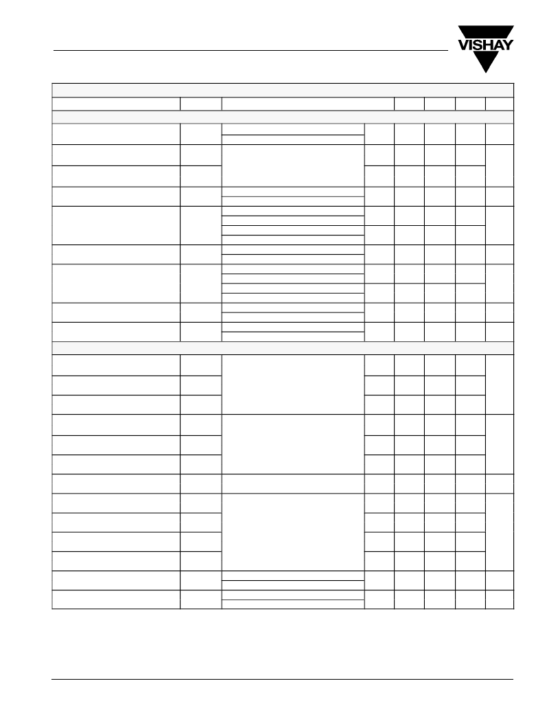
SPECIFICATIONS (T
J
= 25 C UNLESS OTHERWISE NOTED)
Parameter
Symbol
Static
Test Condition
Min
Typ
Max
Unit
Gate Threshold Voltage
V
GS(th)
V
DS
= V
GS
, I
D
= 250 A
V
DS
= V
GS
, I
D
=
250 A
N-Ch
P-Ch
0.6
0.8
1.6
2.2
V
V
DS
Temperature Coefficient
V
DS/Tj
N-Ch
P-Ch
40
40
I
D
= 250 A
mV/ C
V
GS(th)
Temperature Coefficient
V
GS(th)/Tj
N-Ch
P-Ch
N-Ch
P-Ch
N-Ch
P-Ch
N-Ch
P-Ch
N-Ch
P-Ch
N-Ch
P-Ch
N-Ch
P-Ch
N-Ch
P-Ch
N-Ch
P-Ch
3.8
3.4
Gate Body Leakage
Gate-Body Leakage
I
GSS
V
DS
= 0 V, V
GS
=
V
DS
= 0 V, V
GS
=
V
DS
= 40 V, V
GS
= 0 V
V
DS
=
40 V, V
GS
= 0 V
V
DS
= 40 V, V
GS
= 0 V, T
J
= 55 C
V
DS
=
40 V, V
GS
= 0 V, T
J
= 55 C
V
DS
5 V, V
GS
= 10 V
V
DS
5 V, V
GS
=
10 V
V
GS
= 10 V, I
D
= 5.2 A
V
GS
=
10 V, I
D
=
4.5 A
V
GS
= 4.5 V, I
D
= 4.9 A
V
GS
=
4.5 V, I
D
=
3.9 A
V
DS
= 15 V, I
D
= 5.2 A
V
DS
=
15 V, I
D
=
4.5 A
I
S
= 1.7 A, V
GS
= 0 V
I
S
=
1.7 A, V
GS
= 0 V
12 V
16 V
100
100
1
1
10
10
nA
Zero Gate Voltage Drain Current
I
DSS
A
On State Drain Current
On-State Drain Current
a
I
D(on)
20
20
A
0.033
0.045
0.037
0.059
18
13
0.75
0.79
0.040
0.054
0.045
0.072
Drain Source On State Resistance
Drain-Source On-State Resistance
a
r
DS(on)
Forward Transconductance
a
g
fs
S
Diode Forward Voltage
a
V
SD
1.2
1.2
V
Dynamic
b
Input Capacitance
C
iss
N-Channel
N-Ch
P-Ch
N-Ch
P-Ch
N-Ch
P-Ch
700
805
76
120
45
85
V
DS
= 20 V,
V
GS
= 0 V, f = 1 MHz
Output Capacitance
C
oss
P Channel
P-Channel
pF
20 V
= 0 V f = 1 MHz
V
DS
=
20 V,
V
GS
= 0 V, f = 1 MHz
Reverse Transfer Capacitance
C
rss
Total Gate Charge
Q
g
N-Channel
N-Ch
P-Ch
N-Ch
P-Ch
N-Ch
P-Ch
N-Ch
P-Ch
N-Ch
P-Ch
N-Ch
P-Ch
N-Ch
P-Ch
N-Ch
P-Ch
N-Ch
P-Ch
N-Ch
P-Ch
8
9
12
14
V
DS
= 20 V,
V
GS
= 4.5 V, I
D
= 5.2 A
Gate Source Charge
Gate-Source Charge
Q
gs
P Channel
P-Channel
1.5
2
2.4
3.6
1.9
11.5
7
8
11
12
27
74
8
38
25
27
17
17
nC
20 V
4 5 V I
4 5 A
V
DS
=
20 V,
V
GS
=
4.5 V, I
D
=
4.5 A
Gate Drain Charge
Gate-Drain Charge
Q
gd
Gate Resistance
R
g
0.9
5
2.9
18
11
13
17
18
40
110
13
60
40
45
26
26
Turn On Delay Time
Turn-On Delay Time
t
d(on)
N-Channel
Rise Time
t
r
= 15 V, R
= 15
1 A V
1 A, V
GEN
= 10 V R 6
g
= 6
I
D
V
15 V, R
15
ns
Turn Off Delay Time
Turn-Off Delay Time
d( ff)
t
d(off)
P-Channel
V
=
15 V,
= 15
1 A V
1 A, V
GEN
=
10 V, R
= 6
I
D
10 V R 6
Fall Time
t
f
Source-Drain
Reverse Recovery Time
t
rr
I
F
= 1.7 A, di/dt = 100 A/ s
I
F
=
1.7 A, di/dt = 100 A/ s
I
F
= 1.7 A, di/dt = 100 A/ s
I
F
=
1.7 A, di/dt = 100 A/ s
ns
Body Diode
Reverse Recovery Charge
Q
rr
nC
Notes
a.
b.
Pulse test; pulse width
300 s, duty cycle
2%.
Guaranteed by design, not subject to production testing.
Stresses beyond those listed under “Absolute Maximum Ratings” may cause permanent damage to the device. These are stress ratings only, and functional operation of the
device at these or any other conditions beyond those indicated in the operational sections of the specifications is not implied. Exposure to absolute maximum rating conditions
for extended periods may affect device reliability.
相關(guān)PDF資料 |
PDF描述 |
|---|---|
| 732P | Film Capacitors Metalized Polypropylene, Wrap-and-Fill |
| 732P105X9600L | Film Capacitors Metalized Polypropylene, Wrap-and-Fill |
| 732P106X9200L | Film Capacitors Metalized Polypropylene, Wrap-and-Fill |
| 732P105X9200L | Film Capacitors Metalized Polypropylene, Wrap-and-Fill |
| 732P105X9400L | Film Capacitors Metalized Polypropylene, Wrap-and-Fill |
相關(guān)代理商/技術(shù)參數(shù) |
參數(shù)描述 |
|---|---|
| 73224-28LLA | 制造商:FCI 功能描述:CARDBUS NEXTGEN HDR ASSY2.8MM - Bulk |
| 73224-50LLA | 功能描述:記憶卡連接器 CARD BUS II HDR ASSY RoHS:否 制造商:Yamaichi Electronics 產(chǎn)品:Card Connectors 卡類型:microSD 類型: 節(jié)距: 方向: 安裝風(fēng)格:SMD/SMT 端接類型: 排數(shù): 觸點數(shù)量: 電流額定值:0.5 A 電壓額定值:50 V |
| 7322460033194 | 制造商:DORO 功能描述:TELEPHONE, DECT, COLOUR, SMS |
| 7322460033583 | 制造商:DORO 功能描述:TELEPHONE PROFESSIONAL BLACK |
| 73225 | 制造商:Harris Corporation 功能描述: |
發(fā)布緊急采購,3分鐘左右您將得到回復(fù)。