- 您現(xiàn)在的位置:買賣IC網(wǎng) > PDF目錄68811 > 71M6542G-IGT/F (MAXIM INTEGRATED PRODUCTS INC) SPECIALTY ANALOG CIRCUIT, PQFP100 PDF資料下載
參數(shù)資料
| 型號(hào): | 71M6542G-IGT/F |
| 廠商: | MAXIM INTEGRATED PRODUCTS INC |
| 元件分類: | 模擬信號(hào)調(diào)理 |
| 英文描述: | SPECIALTY ANALOG CIRCUIT, PQFP100 |
| 封裝: | LEAD FREE, LQFP-100 |
| 文件頁(yè)數(shù): | 3/165頁(yè) |
| 文件大?。?/td> | 2208K |
| 代理商: | 71M6542G-IGT/F |
第1頁(yè)第2頁(yè)當(dāng)前第3頁(yè)第4頁(yè)第5頁(yè)第6頁(yè)第7頁(yè)第8頁(yè)第9頁(yè)第10頁(yè)第11頁(yè)第12頁(yè)第13頁(yè)第14頁(yè)第15頁(yè)第16頁(yè)第17頁(yè)第18頁(yè)第19頁(yè)第20頁(yè)第21頁(yè)第22頁(yè)第23頁(yè)第24頁(yè)第25頁(yè)第26頁(yè)第27頁(yè)第28頁(yè)第29頁(yè)第30頁(yè)第31頁(yè)第32頁(yè)第33頁(yè)第34頁(yè)第35頁(yè)第36頁(yè)第37頁(yè)第38頁(yè)第39頁(yè)第40頁(yè)第41頁(yè)第42頁(yè)第43頁(yè)第44頁(yè)第45頁(yè)第46頁(yè)第47頁(yè)第48頁(yè)第49頁(yè)第50頁(yè)第51頁(yè)第52頁(yè)第53頁(yè)第54頁(yè)第55頁(yè)第56頁(yè)第57頁(yè)第58頁(yè)第59頁(yè)第60頁(yè)第61頁(yè)第62頁(yè)第63頁(yè)第64頁(yè)第65頁(yè)第66頁(yè)第67頁(yè)第68頁(yè)第69頁(yè)第70頁(yè)第71頁(yè)第72頁(yè)第73頁(yè)第74頁(yè)第75頁(yè)第76頁(yè)第77頁(yè)第78頁(yè)第79頁(yè)第80頁(yè)第81頁(yè)第82頁(yè)第83頁(yè)第84頁(yè)第85頁(yè)第86頁(yè)第87頁(yè)第88頁(yè)第89頁(yè)第90頁(yè)第91頁(yè)第92頁(yè)第93頁(yè)第94頁(yè)第95頁(yè)第96頁(yè)第97頁(yè)第98頁(yè)第99頁(yè)第100頁(yè)第101頁(yè)第102頁(yè)第103頁(yè)第104頁(yè)第105頁(yè)第106頁(yè)第107頁(yè)第108頁(yè)第109頁(yè)第110頁(yè)第111頁(yè)第112頁(yè)第113頁(yè)第114頁(yè)第115頁(yè)第116頁(yè)第117頁(yè)第118頁(yè)第119頁(yè)第120頁(yè)第121頁(yè)第122頁(yè)第123頁(yè)第124頁(yè)第125頁(yè)第126頁(yè)第127頁(yè)第128頁(yè)第129頁(yè)第130頁(yè)第131頁(yè)第132頁(yè)第133頁(yè)第134頁(yè)第135頁(yè)第136頁(yè)第137頁(yè)第138頁(yè)第139頁(yè)第140頁(yè)第141頁(yè)第142頁(yè)第143頁(yè)第144頁(yè)第145頁(yè)第146頁(yè)第147頁(yè)第148頁(yè)第149頁(yè)第150頁(yè)第151頁(yè)第152頁(yè)第153頁(yè)第154頁(yè)第155頁(yè)第156頁(yè)第157頁(yè)第158頁(yè)第159頁(yè)第160頁(yè)第161頁(yè)第162頁(yè)第163頁(yè)第164頁(yè)第165頁(yè)
100
2008–2011 Teridian Semiconductor Corporation
v1.1
GAIN_ADJ2 provides compensation for the remotely connected IB shunt current sensor and compensates
for the 71M6x01 VREF. The designer may optionally add compensation for the shunt connected to the
71M6x01 into the PPMC and PPMC2 coefficients for this channel.
Table 73: GAIN_ADJn Compensation Channels
Gain Adjustment Output
CE RAM Address
71M6541D/F
71M6542F
GAIN_ADJ0
0x40
VA
VA, VB
GAIN_ADJ1
0x41
IA
GAIN_ADJ2
0x42
IB
In the demonstration code, temperature compensation behavior is determined by the values stored in the
PPMC and PPMC2 coefficients, which are setup by the MPU demo code at initialization time from values
that are previously stored in EEPROM.
To disable temperature compensation in the demonstration code, PPMC and PPMC2 are both set to zero
for each of the three GAIN_ADJn channels. To enable temperature compensation, the PPMC and PPMC2
coefficients are set with values that match the expected temperature variation of the corresponding
channel.
For VREF compensation, both the linear coefficient PPMC and the quadratic coefficient PPMC2, are
determined for the 71M654x as described in 4.7.2 Temperature Coefficients for the 71M654x. For
information on determining the PPMC and PPMC2 coefficients for the 71M6x01 VREF, refer to the
71M6xxx Data Sheet.
The compensation for the external error sources is accomplished by summing the PPMC value
associated with VREF with the PPMC value associated with the external error source to obtain the final
PPMC value for the sensor channel. Similarly, the PPMC2 value associated with VREF is summed with
the PPMC2 value associated with the external error source.
To determine the contribution of the current shunt sensor to the PPMC and PPMC2 coefficients, the
designer must either know the temperature coefficients of the shunt from its data sheet or obtain it by
laboratory measurement. The designer must consider component variation across mass production to
ensure that the product will meet its accuracy requirement across production.
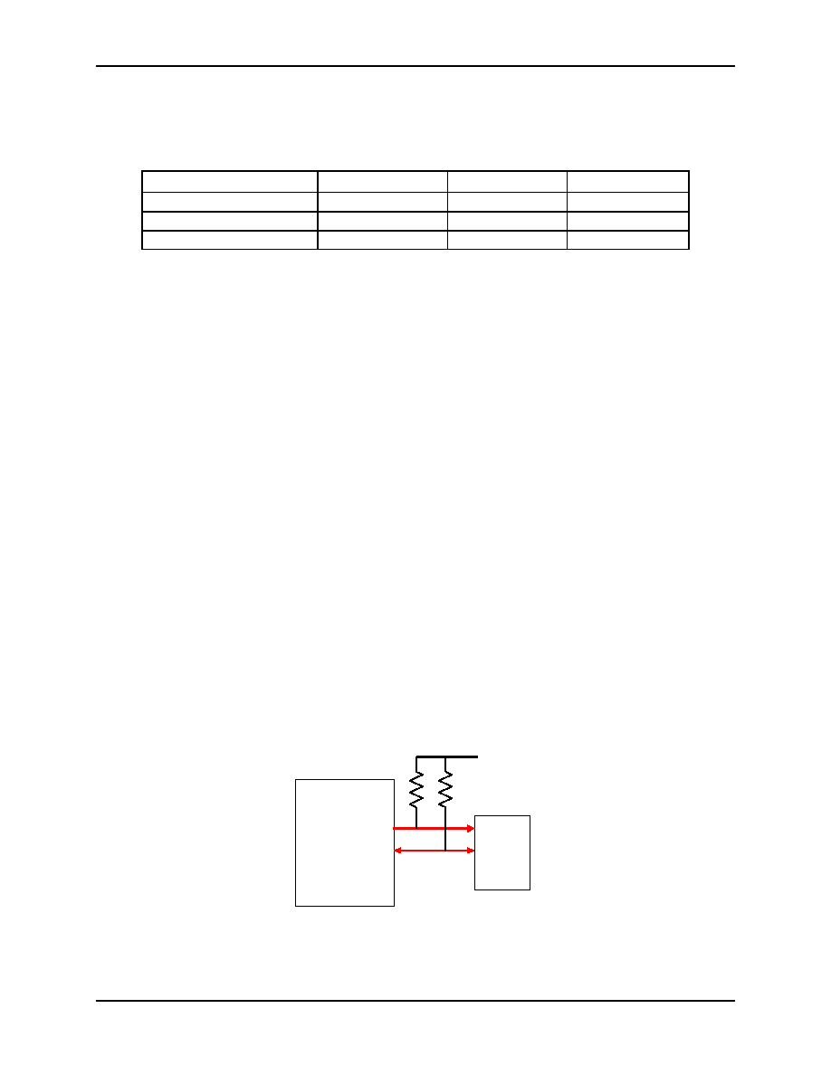
4.8
Connecting I
2C EEPROMs
I
2C EEPROMs or other I2C compatible devices should be connected to the DIO pins SEGDIO2 and
SEGDIO3, as shown in Figure 39.
Pull-up resistors of roughly 10 k
to V3P3D (to ensure operation in BRN mode) should be used for both
SDCK and SDATA signals. The DIO_EEX[1:0] (I/O RAM 0x2456[7:6]) field in I/O RAM must be set to 01
in order to convert the DIO pins SEGDIO2 and SEGDIO3 to I
2C pins SDCK and SDATA.
Figure 39: I
2C EEPROM Connection
SEGDIO2/SDCK
EEPROM
SDCK
SDATA
V3P3D
10 k
Ω
10 k
Ω
71M654x
SEGDIO3/SDATA
相關(guān)PDF資料 |
PDF描述 |
|---|---|
| 71M6541G-IGT/F | SPECIALTY ANALOG CIRCUIT, PQFP64 |
| 71M6541F-IGT/F | SPECIALTY ANALOG CIRCUIT, PQFP64 |
| 71M6543F-IGT/F | SPECIALTY ANALOG CIRCUIT, PQFP100 |
| 71M6543H-IGTR/F | SPECIALTY ANALOG CIRCUIT, PQFP100 |
| 71M6543F-IGTR/F | SPECIALTY ANALOG CIRCUIT, PQFP100 |
相關(guān)代理商/技術(shù)參數(shù) |
參數(shù)描述 |
|---|---|
| 71M6542G-IGTR/F | 制造商:Maxim Integrated Products 功能描述:- Tape and Reel |
| 71M6542GT-IGT/F | 制造商:Maxim Integrated Products 功能描述:1-PHASE, 128KB, PRES TEMP SENSOR - Bulk |
| 71M6542GT-IGTR/F | 制造商:Maxim Integrated Products 功能描述:1-PHASE, 128KB, PRES TEMP SENSOR - Tape and Reel |
| 71M6543F | 制造商:MAXIM 制造商全稱:Maxim Integrated Products 功能描述:Selectable Gain of 1 or 8 for One Current Energy Meter ICs Metrology Compensation |
| 71M6543F-DB | 功能描述:開(kāi)發(fā)板和工具包 - 8051 71M6543 Eval Kit RoHS:否 制造商:Silicon Labs 產(chǎn)品:Development Kits 工具用于評(píng)估:C8051F960, Si7005 核心: 接口類型:USB 工作電源電壓: |
發(fā)布緊急采購(gòu),3分鐘左右您將得到回復(fù)。