- 您現(xiàn)在的位置:買賣IC網(wǎng) > PDF目錄68811 > 71M6542F-IGT/F (MAXIM INTEGRATED PRODUCTS INC) SPECIALTY ANALOG CIRCUIT, PQFP100 PDF資料下載
參數(shù)資料
| 型號: | 71M6542F-IGT/F |
| 廠商: | MAXIM INTEGRATED PRODUCTS INC |
| 元件分類: | 模擬信號調(diào)理 |
| 英文描述: | SPECIALTY ANALOG CIRCUIT, PQFP100 |
| 封裝: | LEAD FREE, LQFP-100 |
| 文件頁數(shù): | 77/165頁 |
| 文件大小: | 2208K |
| 代理商: | 71M6542F-IGT/F |
第1頁第2頁第3頁第4頁第5頁第6頁第7頁第8頁第9頁第10頁第11頁第12頁第13頁第14頁第15頁第16頁第17頁第18頁第19頁第20頁第21頁第22頁第23頁第24頁第25頁第26頁第27頁第28頁第29頁第30頁第31頁第32頁第33頁第34頁第35頁第36頁第37頁第38頁第39頁第40頁第41頁第42頁第43頁第44頁第45頁第46頁第47頁第48頁第49頁第50頁第51頁第52頁第53頁第54頁第55頁第56頁第57頁第58頁第59頁第60頁第61頁第62頁第63頁第64頁第65頁第66頁第67頁第68頁第69頁第70頁第71頁第72頁第73頁第74頁第75頁第76頁當(dāng)前第77頁第78頁第79頁第80頁第81頁第82頁第83頁第84頁第85頁第86頁第87頁第88頁第89頁第90頁第91頁第92頁第93頁第94頁第95頁第96頁第97頁第98頁第99頁第100頁第101頁第102頁第103頁第104頁第105頁第106頁第107頁第108頁第109頁第110頁第111頁第112頁第113頁第114頁第115頁第116頁第117頁第118頁第119頁第120頁第121頁第122頁第123頁第124頁第125頁第126頁第127頁第128頁第129頁第130頁第131頁第132頁第133頁第134頁第135頁第136頁第137頁第138頁第139頁第140頁第141頁第142頁第143頁第144頁第145頁第146頁第147頁第148頁第149頁第150頁第151頁第152頁第153頁第154頁第155頁第156頁第157頁第158頁第159頁第160頁第161頁第162頁第163頁第164頁第165頁
v1.1
2008–2011 Teridian Semiconductor Corporation
19
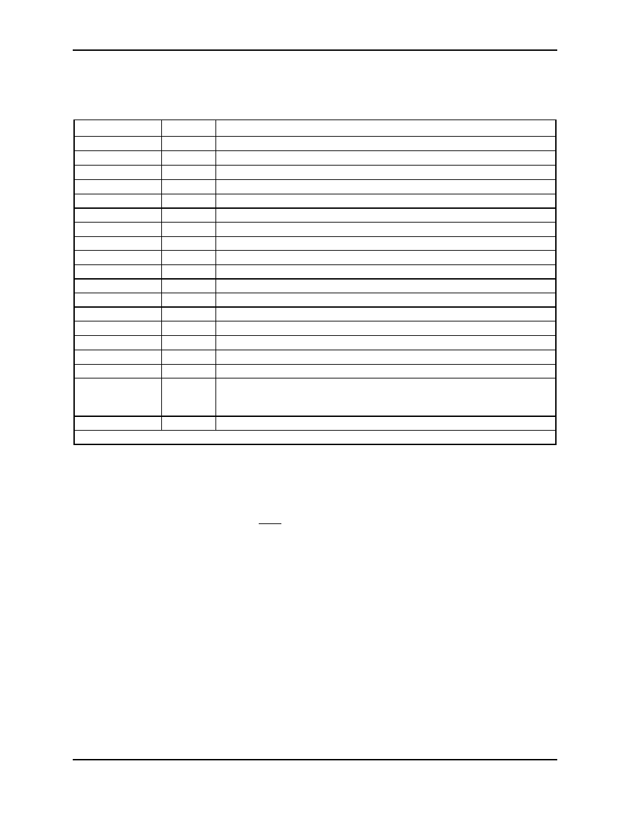
Table 4 summarizes the I/O RAM registers used for configuring the multiplexer, signals pins, and ADC.
All listed registers are 0 after reset and wake from battery modes, and are readable and writable.
Table 4: Multiplexer and ADC Configuration Bits
Name
Location
Description
MUX0_SEL[3:0]
2105[3:0]
Selects the ADC input converted during time slot 0.
MUX1_SEL[3:0]
2105[7:4]
Selects the ADC input converted during time slot 1.
MUX2_SEL[3:0]
2104[3:0]
Selects the ADC input converted during time slot 2.
MUX3_SEL[3:0]
2104[7:4]
Selects the ADC input converted during time slot 3.
MUX4_SEL[3:0]
2103[3:0]
Selects the ADC input converted during time slot 4.
MUX5_SEL[3:0]
2103[7:4]
Selects the ADC input converted during time slot 5.
MUX6_SEL[3:0]
2102[3:0]
Selects the ADC input converted during time slot 6.
MUX7_SEL[3:0]
2102[7:0]
Selects the ADC input converted during time slot 7.
MUX8_SEL[3:0]
2101[3:0]
Selects the ADC input converted during time slot 8.
MUX9_SEL[3:0]
2101[7:0]
Selects the ADC input converted during time slot 9.
MUX10_SEL[3:0]
2100[3:0]
Selects the ADC input converted during time slot 10.
ADC_DIV
2200[5]
Controls the rate of the ADC and FIR clocks.
MUX_DIV[3:0]
2100[7:4]
The number of ADC time slots in each multiplexer frame (maximum = 11).
PLL_FAST
2200[4]
Controls the speed of the PLL and MCK.
FIR_LEN[1:0]
210C[1]
Determines the number of ADC cycles in the ADC decimation FIR filter.
DIFFA_E
210C[4]
Enables the differential configuration for analog input pins IAP-IAN.
DIFFB_E
210C[5]
Enables the differential configuration for analog input pins IBP-IBN.
RMT_E
2709[3]
Enables the remote sensor interface transforming pins IBP-IBN into a
digital balanced differential pair for communications with the 71M6x01
sensor.
PRE_E
2704[5]
Enables the 8x pre-amplifier.
2.2.3
Delay Compensation
When measuring the energy of a phase (i.e., Wh and VARh) in a service, the voltage and current for that
phase must be sampled at the same instant. Otherwise, the phase difference,
Ф, introduces errors.
o
delay
o
delay
f
t
T
t
360
=
=
φ
Where f is the frequency of the input signal, T = 1/f and tdelay is the sampling delay between current and
voltage.
Traditionally, sampling is accomplished by using two A/D converters per phase (one for voltage and the
other one for current) controlled to sample simultaneously. Teridian’s Single-Converter Technology,
however, exploits the 32-bit signal processing capability of its CE to implement “constant delay” all-pass
filters. The all-pass filter corrects for the conversion time difference between the voltage and the
corresponding current samples that are obtained with a single multiplexed A/D converter.
The “constant delay” all-pass filter provides a broad-band delay 360
o –
θ, which is precisely matched to
the difference in sample time between the voltage and the current of a given phase. This digital filter
does not affect the amplitude of the signal, but provides a precisely controlled phase response.
The recommended ADC multiplexer sequence samples the current first, immediately followed by
sampling of the corresponding phase voltage, thus the voltage is delayed by a phase angle
Ф relative to
the current. The delay compensation implemented in the CE aligns the voltage samples with their
corresponding current samples by first delaying the current samples by one full sample interval (i.e.,
360
o), then routing the voltage samples through the all-pass filter, thus delaying the voltage samples by
相關(guān)PDF資料 |
PDF描述 |
|---|---|
| 71M6542G-IGTR/F | SPECIALTY ANALOG CIRCUIT, PQFP100 |
| 71M6541G-IGTR/F | SPECIALTY ANALOG CIRCUIT, PQFP64 |
| 71M6541F-IGTR/F | SPECIALTY ANALOG CIRCUIT, PQFP64 |
| 71M6541D-IGTR/F | SPECIALTY ANALOG CIRCUIT, PQFP64 |
| 71M6542F-IGTR/F | SPECIALTY ANALOG CIRCUIT, PQFP100 |
相關(guān)代理商/技術(shù)參數(shù) |
參數(shù)描述 |
|---|---|
| 71M6542F-IGTR/F | 功能描述:計量片上系統(tǒng) - SoC Precision Energy Meter IC RoHS:否 制造商:Maxim Integrated 核心:80515 MPU 處理器系列:71M6511 類型:Metering SoC 最大時鐘頻率:70 Hz 程序存儲器大小:64 KB 數(shù)據(jù) RAM 大小:7 KB 接口類型:UART 可編程輸入/輸出端數(shù)量:12 片上 ADC: 安裝風(fēng)格:SMD/SMT 封裝 / 箱體:LQFP-64 封裝:Reel |
| 71M6542FT-IGT/F | 制造商:Maxim Integrated Products 功能描述:1-PHASE SOC 128KB WITH PREC TEMP SENSOR - Rail/Tube |
| 71M6542FT-IGTR/F | 制造商:Maxim Integrated Products 功能描述:1-PHASE SOC, 64KB FLASH, PRES TEMP SENSOR - Tape and Reel |
| 71M6542G | 制造商:未知廠家 制造商全稱:未知廠家 功能描述:71M6541D/71M6541F/71M6541G/71M6542F/71M6542G 是 TeridianTM 的第4 代高集成度單相電表SoC |
| 71M6542G-IGT/F | 功能描述:計量片上系統(tǒng) - SoC 1-Phase Metering SOC with 128KB Flash RoHS:否 制造商:Maxim Integrated 核心:80515 MPU 處理器系列:71M6511 類型:Metering SoC 最大時鐘頻率:70 Hz 程序存儲器大小:64 KB 數(shù)據(jù) RAM 大小:7 KB 接口類型:UART 可編程輸入/輸出端數(shù)量:12 片上 ADC: 安裝風(fēng)格:SMD/SMT 封裝 / 箱體:LQFP-64 封裝:Reel |
發(fā)布緊急采購,3分鐘左右您將得到回復(fù)。