- 您現(xiàn)在的位置:買賣IC網(wǎng) > PDF目錄68811 > 71M6541F-IGT/F (MAXIM INTEGRATED PRODUCTS INC) SPECIALTY ANALOG CIRCUIT, PQFP64 PDF資料下載
參數(shù)資料
| 型號(hào): | 71M6541F-IGT/F |
| 廠商: | MAXIM INTEGRATED PRODUCTS INC |
| 元件分類: | 模擬信號(hào)調(diào)理 |
| 英文描述: | SPECIALTY ANALOG CIRCUIT, PQFP64 |
| 封裝: | LEAD FREE, LQFP-64 |
| 文件頁(yè)數(shù): | 91/165頁(yè) |
| 文件大小: | 2208K |
| 代理商: | 71M6541F-IGT/F |
第1頁(yè)第2頁(yè)第3頁(yè)第4頁(yè)第5頁(yè)第6頁(yè)第7頁(yè)第8頁(yè)第9頁(yè)第10頁(yè)第11頁(yè)第12頁(yè)第13頁(yè)第14頁(yè)第15頁(yè)第16頁(yè)第17頁(yè)第18頁(yè)第19頁(yè)第20頁(yè)第21頁(yè)第22頁(yè)第23頁(yè)第24頁(yè)第25頁(yè)第26頁(yè)第27頁(yè)第28頁(yè)第29頁(yè)第30頁(yè)第31頁(yè)第32頁(yè)第33頁(yè)第34頁(yè)第35頁(yè)第36頁(yè)第37頁(yè)第38頁(yè)第39頁(yè)第40頁(yè)第41頁(yè)第42頁(yè)第43頁(yè)第44頁(yè)第45頁(yè)第46頁(yè)第47頁(yè)第48頁(yè)第49頁(yè)第50頁(yè)第51頁(yè)第52頁(yè)第53頁(yè)第54頁(yè)第55頁(yè)第56頁(yè)第57頁(yè)第58頁(yè)第59頁(yè)第60頁(yè)第61頁(yè)第62頁(yè)第63頁(yè)第64頁(yè)第65頁(yè)第66頁(yè)第67頁(yè)第68頁(yè)第69頁(yè)第70頁(yè)第71頁(yè)第72頁(yè)第73頁(yè)第74頁(yè)第75頁(yè)第76頁(yè)第77頁(yè)第78頁(yè)第79頁(yè)第80頁(yè)第81頁(yè)第82頁(yè)第83頁(yè)第84頁(yè)第85頁(yè)第86頁(yè)第87頁(yè)第88頁(yè)第89頁(yè)第90頁(yè)當(dāng)前第91頁(yè)第92頁(yè)第93頁(yè)第94頁(yè)第95頁(yè)第96頁(yè)第97頁(yè)第98頁(yè)第99頁(yè)第100頁(yè)第101頁(yè)第102頁(yè)第103頁(yè)第104頁(yè)第105頁(yè)第106頁(yè)第107頁(yè)第108頁(yè)第109頁(yè)第110頁(yè)第111頁(yè)第112頁(yè)第113頁(yè)第114頁(yè)第115頁(yè)第116頁(yè)第117頁(yè)第118頁(yè)第119頁(yè)第120頁(yè)第121頁(yè)第122頁(yè)第123頁(yè)第124頁(yè)第125頁(yè)第126頁(yè)第127頁(yè)第128頁(yè)第129頁(yè)第130頁(yè)第131頁(yè)第132頁(yè)第133頁(yè)第134頁(yè)第135頁(yè)第136頁(yè)第137頁(yè)第138頁(yè)第139頁(yè)第140頁(yè)第141頁(yè)第142頁(yè)第143頁(yè)第144頁(yè)第145頁(yè)第146頁(yè)第147頁(yè)第148頁(yè)第149頁(yè)第150頁(yè)第151頁(yè)第152頁(yè)第153頁(yè)第154頁(yè)第155頁(yè)第156頁(yè)第157頁(yè)第158頁(yè)第159頁(yè)第160頁(yè)第161頁(yè)第162頁(yè)第163頁(yè)第164頁(yè)第165頁(yè)
v1.1
2008–2011 Teridian Semiconductor Corporation
31
2.4
80515 MPU Core
The 71M6541D/F and 71M6542F include an 80515 MPU (8-bit, 8051-compatible) that processes most
instructions in one clock cycle. Using a 4.9 MHz clock results in a processing throughput of 4.9 MIPS. The
80515 architecture eliminates redundant bus states and implements parallel execution of fetch and execution
phases. Normally, a machine cycle is aligned with a memory fetch, therefore, most of the 1-byte instructions
are performed in a single machine cycle (MPU clock cycle). This leads to an 8x average performance
improvement (in terms of MIPS) over the Intel
8051 device running at the same clock frequency.
Table 9 shows the CKMPU frequency as a function of the MCK clock (19.6608 MHz) divided by the MPU
clock divider which is set in the I/O RAM control field MPU_DIV[2:0] (I/O RAM 0x2200[2:0]). Actual processor
clocking speed can be adjusted to the total processing demand of the application (metering calculations,
AMR management, memory management, LCD driver management and I/O management) using
MPU_DIV[2:0], as shown in Table 9.
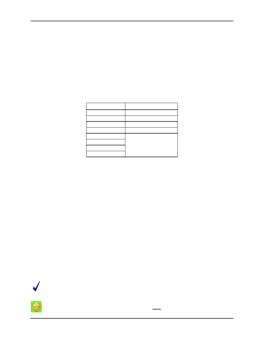
Table 9: CKMPU Clock Frequencies
MPU_DIV [2:0]
CKMPU Frequency
000
4.9152 MHz
001
2.4576 MHz
010
1.2288 MHz
011
614.4 kHz
100
307.2 kHz
101
110
111
Typical measurement and metering functions based on the results provided by the internal 32-bit compute
engine (CE) are available for the MPU as part of the Teridian standard library. Teridian provides
demonstration source code to help reduce the design cycle.
2.4.1
Memory Organization and Addressing
The 80515 MPU core incorporates the Harvard architecture with separate code and data spaces. Memory
organization in the 80515 is similar to that of the industry standard 8051. There are three memory areas:
Program memory (Flash, shared by MPU and CE), external RAM (Data RAM, shared by the CE and MPU,
Configuration or I/O RAM), and internal data memory (Internal RAM). Table 10 shows the memory map.
Program Memory
The 80515 can address up to 64 KB of program memory space (0x0000 to 0xFFFF). Program memory is
read when the MPU fetches instructions or performs a MOVC operation.
After reset, the MPU starts program execution from program memory location 0x0000. The lower part of
the program memory includes reset and interrupt vectors. The interrupt vectors are spaced at 8-byte
intervals, starting from 0x0003.
MPU External Data Memory (XRAM)
Both internal and external memory is physically located on the 71M654x device. The external memory
referred in this documentation is only external to the 80515 MPU core.
3 KB of RAM starting at address 0x0000 is shared by the CE and MPU. The CE normally uses the first
1 KB, leaving 2 KB for the MPU. Different versions of the CE code use varying amounts. Consult the
documentation for the specific code version being used for the exact limit.
If the MPU overwrites the CE’s working RAM, the CE’s output may be corrupted. If the CE is
disabled, the first 0x40 bytes of RAM are still unusable while MUX_DIV[3:0]
≠ 0 because the
71M654x ADC writes to these locations. Setting MUX_DIV[3:0] = 0 disables the ADC output
preventing the CE from writing the first 0x40 bytes of RAM.
In addition, MUXn_SEL[3:0] values must be written only after writing MUX_DIV[3:0].
相關(guān)PDF資料 |
PDF描述 |
|---|---|
| 71M6543F-IGT/F | SPECIALTY ANALOG CIRCUIT, PQFP100 |
| 71M6543H-IGTR/F | SPECIALTY ANALOG CIRCUIT, PQFP100 |
| 71M6543F-IGTR/F | SPECIALTY ANALOG CIRCUIT, PQFP100 |
| 71M6543H-IGT/F | SPECIALTY ANALOG CIRCUIT, PQFP100 |
| 71M6543G-IGTR/F | SPECIALTY ANALOG CIRCUIT, PQFP100 |
相關(guān)代理商/技術(shù)參數(shù) |
參數(shù)描述 |
|---|---|
| 71M6541F-IGTR/F | 功能描述:計(jì)量片上系統(tǒng) - SoC Precision Energy Meter IC RoHS:否 制造商:Maxim Integrated 核心:80515 MPU 處理器系列:71M6511 類型:Metering SoC 最大時(shí)鐘頻率:70 Hz 程序存儲(chǔ)器大小:64 KB 數(shù)據(jù) RAM 大小:7 KB 接口類型:UART 可編程輸入/輸出端數(shù)量:12 片上 ADC: 安裝風(fēng)格:SMD/SMT 封裝 / 箱體:LQFP-64 封裝:Reel |
| 71M6541FT-IGT/F | 制造商:Maxim Integrated Products 功能描述:1-PHASE SOC, 64KB FLASH, PRES TEMP SENSOR - Rail/Tube |
| 71M6541FT-IGTR/F | 制造商:Maxim Integrated Products 功能描述:1-PHASE SOC, 64KB FLASH, PRES TEMP SENSOR - Tape and Reel |
| 71M6541G | 制造商:未知廠家 制造商全稱:未知廠家 功能描述:71M6541D/71M6541F/71M6541G/71M6542F/71M6542G 是 TeridianTM 的第4 代高集成度單相電表SoC |
| 71M6541G-IGT/F | 功能描述:計(jì)量片上系統(tǒng) - SoC 71M6541G-IGT/F RoHS:否 制造商:Maxim Integrated 核心:80515 MPU 處理器系列:71M6511 類型:Metering SoC 最大時(shí)鐘頻率:70 Hz 程序存儲(chǔ)器大小:64 KB 數(shù)據(jù) RAM 大小:7 KB 接口類型:UART 可編程輸入/輸出端數(shù)量:12 片上 ADC: 安裝風(fēng)格:SMD/SMT 封裝 / 箱體:LQFP-64 封裝:Reel |
發(fā)布緊急采購(gòu),3分鐘左右您將得到回復(fù)。