- 您現(xiàn)在的位置:買賣IC網(wǎng) > PDF目錄68811 > 71M6531D-IM/F (TERIDIAN SEMICONDUCTOR CORP) 1-CHANNEL POWER SUPPLY MANAGEMENT CKT, QCC68 PDF資料下載
參數(shù)資料
| 型號(hào): | 71M6531D-IM/F |
| 廠商: | TERIDIAN SEMICONDUCTOR CORP |
| 元件分類: | 電源管理 |
| 英文描述: | 1-CHANNEL POWER SUPPLY MANAGEMENT CKT, QCC68 |
| 封裝: | LEAD FREE, QFN-68 |
| 文件頁(yè)數(shù): | 26/120頁(yè) |
| 文件大小: | 2477K |
| 代理商: | 71M6531D-IM/F |
第1頁(yè)第2頁(yè)第3頁(yè)第4頁(yè)第5頁(yè)第6頁(yè)第7頁(yè)第8頁(yè)第9頁(yè)第10頁(yè)第11頁(yè)第12頁(yè)第13頁(yè)第14頁(yè)第15頁(yè)第16頁(yè)第17頁(yè)第18頁(yè)第19頁(yè)第20頁(yè)第21頁(yè)第22頁(yè)第23頁(yè)第24頁(yè)第25頁(yè)當(dāng)前第26頁(yè)第27頁(yè)第28頁(yè)第29頁(yè)第30頁(yè)第31頁(yè)第32頁(yè)第33頁(yè)第34頁(yè)第35頁(yè)第36頁(yè)第37頁(yè)第38頁(yè)第39頁(yè)第40頁(yè)第41頁(yè)第42頁(yè)第43頁(yè)第44頁(yè)第45頁(yè)第46頁(yè)第47頁(yè)第48頁(yè)第49頁(yè)第50頁(yè)第51頁(yè)第52頁(yè)第53頁(yè)第54頁(yè)第55頁(yè)第56頁(yè)第57頁(yè)第58頁(yè)第59頁(yè)第60頁(yè)第61頁(yè)第62頁(yè)第63頁(yè)第64頁(yè)第65頁(yè)第66頁(yè)第67頁(yè)第68頁(yè)第69頁(yè)第70頁(yè)第71頁(yè)第72頁(yè)第73頁(yè)第74頁(yè)第75頁(yè)第76頁(yè)第77頁(yè)第78頁(yè)第79頁(yè)第80頁(yè)第81頁(yè)第82頁(yè)第83頁(yè)第84頁(yè)第85頁(yè)第86頁(yè)第87頁(yè)第88頁(yè)第89頁(yè)第90頁(yè)第91頁(yè)第92頁(yè)第93頁(yè)第94頁(yè)第95頁(yè)第96頁(yè)第97頁(yè)第98頁(yè)第99頁(yè)第100頁(yè)第101頁(yè)第102頁(yè)第103頁(yè)第104頁(yè)第105頁(yè)第106頁(yè)第107頁(yè)第108頁(yè)第109頁(yè)第110頁(yè)第111頁(yè)第112頁(yè)第113頁(yè)第114頁(yè)第115頁(yè)第116頁(yè)第117頁(yè)第118頁(yè)第119頁(yè)第120頁(yè)
FDS 6531/6532 005
Data Sheet 71M6531D/F-71M6532D/F
v1.3
2005-2010 TERIDIAN Semiconductor Corporation
13
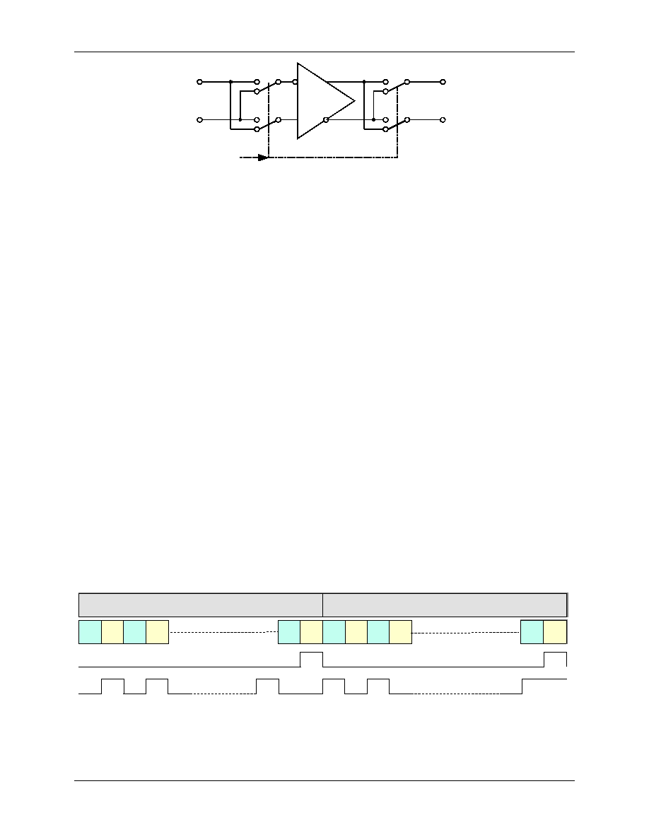
Figure 3: General Topology of a Chopped Amplifier
It is assumed that an offset voltage Voff appears at the positive amplifier input. With all switches, as
controlled by CROSS, in the A position, the output voltage is:
Voutp – Voutn = G (Vinp + Voff – Vinn) = G (Vinp – Vinn) + G Voff
With all switches set to the B position by applying the inverted CROSS signal, the output voltage is:
Voutn – Voutp = G (Vinn – Vinp + Voff) = G (Vinn – Vinp) + G Voff, or
Voutp – Voutn = G (Vinp – Vinn) - G Voff
Thus, when CROSS is toggled, e.g. after each multiplexer cycle, the offset will alternately appear on the
output as positive and negative, which results in the offset effectively being eliminated, regardless of its
polarity or magnitude.
When CROSS is high, the connection of the amplifier input devices is reversed. This preserves the overall
polarity of that amplifier gain; it inverts its input offset. By alternately reversing the connection, the
amplifier’s offset is averaged to zero. This removes the most significant long-term drift mechanism in the
voltage reference. The CHOP_E[1:0] field controls the behavior of CROSS. The CROSS signal will reverse
the amplifier connection in the voltage reference in order to negate the effects of its offset. On the first
CK32 rising edge after the last multiplexer state of its sequence, the multiplexer will wait one additional
CK32 cycle before beginning a new frame. At the beginning of this cycle, the value of CROSS will be
updated according to the CHOP_E[1:0] field. The extra CK32 cycle allows time for the chopped VREF to
settle. During this cycle, MUXSYNC is held high. The leading edge of MUXSYNC initiates a pass
through the CE program sequence. The beginning of the sequence is the serial readout of the four RTM
words.
CHOP_E[1:0] has four states: positive, reverse and two toggle states. In the positive state, CHOP_E[1:0]
= 01, CROSS and CHOP_CLK are held low. In the reverse state, CHOP_E[1:0] = 10, CROSS and
CHOP_CLK are held high. In the first toggle state, CHOP_E[1:0] = 00, CROSS is automatically toggled
near the end of each multiplexer frame and an ALT frame is forced during the last multiplexer frame in each
SUM cycle. It is desirable that CROSS take on alternate values during each ALT frame. For this reason,
if CHOP_E[1:0] = 00, CROSS will not toggle at the end of the multiplexer frame immediately preceding
the ALT frame in each accumulation interval.
Figure 4: CROSS Signal with CHOP_E[1:0] = 00
Figure 4 shows CROSS over two accumulation interval when CHOP_E[1:0] = 00: At the end of the first
interval, CROSS is low, at the end of the second interval, CROSS is high. The offset error for the two
temperature measurements taken during the ALT multiplexer frames will be averaged to zero. Note that
G
-
+
V
inp
V
outp
V
outn
V
inn
CROSS
A
B
A
B
A
B
A
B
Multiplexer frames
Accumulation interval n
Accumulation interval n+1
2
4
3
2519 2520
1
2
4
3
2519 2520
1
Alternative MUX cycle
Multiplexer frames
Alternative MUX cycle
CROSS
相關(guān)PDF資料 |
PDF描述 |
|---|---|
| 71M6532F-IGTR/F | 1-CHANNEL POWER SUPPLY MANAGEMENT CKT, PQFP100 |
| 71M6534-IGT/F | SPECIALTY ANALOG CIRCUIT, PQFP120 |
| 71M6534H-IGTR/F | SPECIALTY ANALOG CIRCUIT, PQFP120 |
| 71M6533H-IGTR/F | SPECIALTY ANALOG CIRCUIT, PQFP100 |
| 71M6534-IGTR/F | SPECIALTY ANALOG CIRCUIT, PQFP120 |
相關(guān)代理商/技術(shù)參數(shù) |
參數(shù)描述 |
|---|---|
| 71M6531D-IMR/F | 功能描述:計(jì)量片上系統(tǒng) - SoC Residential Energy Meter IC RoHS:否 制造商:Maxim Integrated 核心:80515 MPU 處理器系列:71M6511 類型:Metering SoC 最大時(shí)鐘頻率:70 Hz 程序存儲(chǔ)器大小:64 KB 數(shù)據(jù) RAM 大小:7 KB 接口類型:UART 可編程輸入/輸出端數(shù)量:12 片上 ADC: 安裝風(fēng)格:SMD/SMT 封裝 / 箱體:LQFP-64 封裝:Reel |
| 71M6531D-IMR/F1 | 功能描述:計(jì)量片上系統(tǒng) - SoC RoHS:否 制造商:Maxim Integrated 核心:80515 MPU 處理器系列:71M6511 類型:Metering SoC 最大時(shí)鐘頻率:70 Hz 程序存儲(chǔ)器大小:64 KB 數(shù)據(jù) RAM 大小:7 KB 接口類型:UART 可編程輸入/輸出端數(shù)量:12 片上 ADC: 安裝風(fēng)格:SMD/SMT 封裝 / 箱體:LQFP-64 封裝:Reel |
| 71M6531D-IMR/F2 | 功能描述:計(jì)量片上系統(tǒng) - SoC Residential Energy Meter IC RoHS:否 制造商:Maxim Integrated 核心:80515 MPU 處理器系列:71M6511 類型:Metering SoC 最大時(shí)鐘頻率:70 Hz 程序存儲(chǔ)器大小:64 KB 數(shù)據(jù) RAM 大小:7 KB 接口類型:UART 可編程輸入/輸出端數(shù)量:12 片上 ADC: 安裝風(fēng)格:SMD/SMT 封裝 / 箱體:LQFP-64 封裝:Reel |
| 71M6531F | 制造商:TERIDIAN 制造商全稱:TERIDIAN 功能描述:Energy Meter IC |
| 71M6531F-DB | 功能描述:開發(fā)板和工具包 - 8051 71M6531F Demo Brd RoHS:否 制造商:Silicon Labs 產(chǎn)品:Development Kits 工具用于評(píng)估:C8051F960, Si7005 核心: 接口類型:USB 工作電源電壓: |
發(fā)布緊急采購(gòu),3分鐘左右您將得到回復(fù)。