- 您現(xiàn)在的位置:買賣IC網(wǎng) > PDF目錄222673 > 5962-8959834M7A (MICROSS COMPONENTS) 128K X 8 STANDARD SRAM, 45 ns, CDSO32 PDF資料下載
參數(shù)資料
| 型號(hào): | 5962-8959834M7A |
| 廠商: | MICROSS COMPONENTS |
| 元件分類: | SRAM |
| 英文描述: | 128K X 8 STANDARD SRAM, 45 ns, CDSO32 |
| 封裝: | CERAMIC, SOJ-32 |
| 文件頁(yè)數(shù): | 13/17頁(yè) |
| 文件大?。?/td> | 212K |
| 代理商: | 5962-8959834M7A |
第1頁(yè)第2頁(yè)第3頁(yè)第4頁(yè)第5頁(yè)第6頁(yè)第7頁(yè)第8頁(yè)第9頁(yè)第10頁(yè)第11頁(yè)第12頁(yè)當(dāng)前第13頁(yè)第14頁(yè)第15頁(yè)第16頁(yè)第17頁(yè)
SRAM
MT5C1008
MT5C1008
Rev. 6.8 01/10
Micross Components reserves the right to change products or specications without notice.
5
AC TEST CONDITIONS
Input pulse levels ................................... Vss to 3.0V
Input rise and fall times ....................................... 5ns
Input timing reference levels ............................. 1.5V
Output reference levels ..................................... 1.5V
Output load .............................. See Figures 1 and 2
NOTES
1.
All voltages referenced to V
SS (GND).
2.
-2V for pulse width < 20ns
3.
I
CC is dependent on output loading and cycle rates.
The specied value applies with the outputs
unloaded, and f =
1
Hz.
tRC (MIN)
4.
This parameter is guaranteed but not tested.
5.
Test conditions as specied with the output loading
as shown in Fig. 1 unless otherwise noted.
6.
tLZCE, tLZWE, tLZOE, t HZCE, tHZOE and tHZWE
are specied with CL = 5pF as in Fig. 2. Transition is
measured ±200mV typical from steady state voltage,
allowing for actual tester RC time constant.
7.
At any given temperature and voltage condition,
tHZCE is less than tLZCE, and tHZWE is less than
tLZWE and tHZOE is less than tLZOE.
8.
WE\ is HIGH for READ cycle.
9.
Device is continuously selected. Chip enables and
output enables are held in their active state.
10. Address valid prior to, or coincident with, latest
occurring chip enable.
11. tRC = Read Cycle Time.
12. CE2 timing is the same as CE1\ timing. The
waveform is inverted.
13. Chip enable (CE1\, CE2) and write enable (WE\) can
initiate and terminate a WRITE cycle.
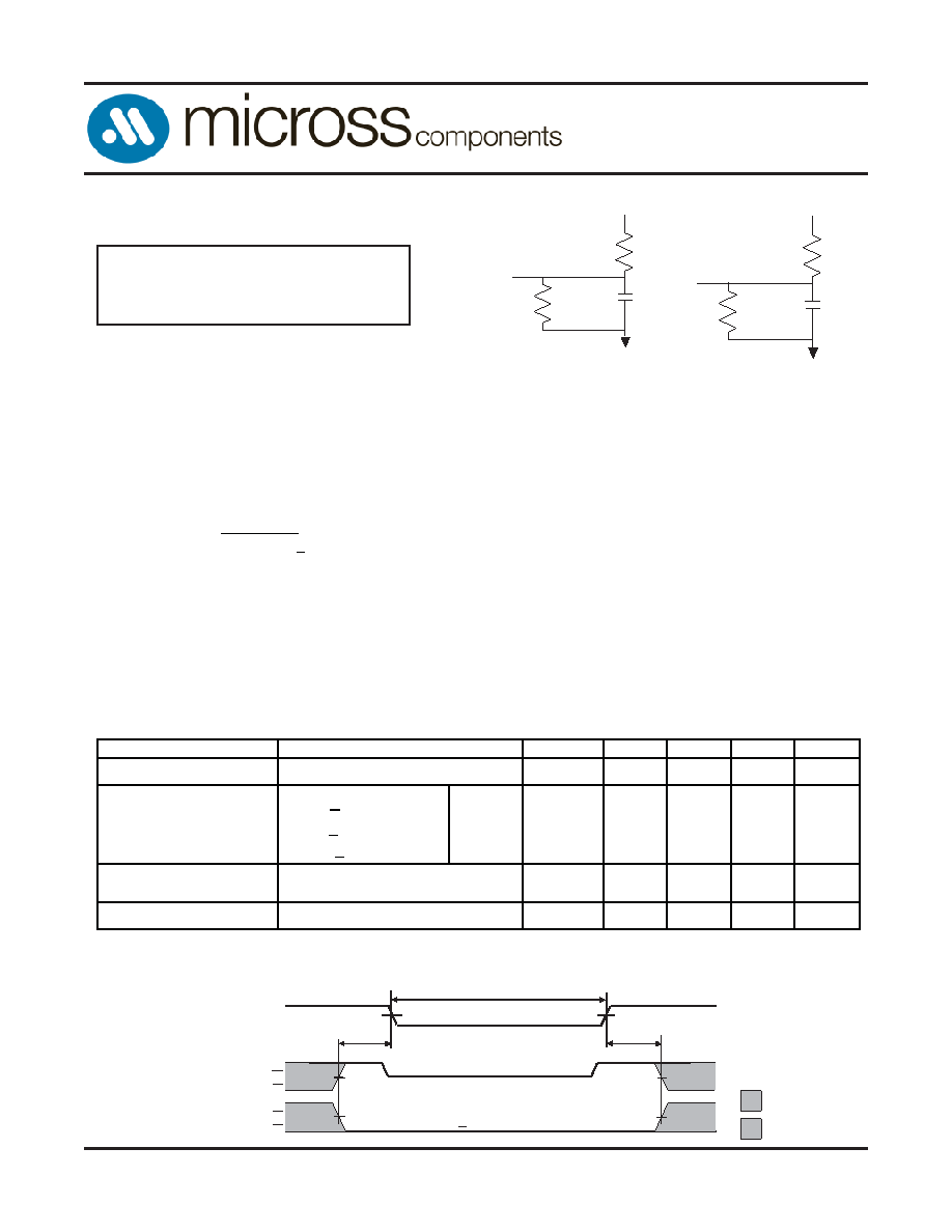
Fig. 1 Output Load
Equivalent
Fig. 2 Output Load
Equivalent
DATA RETENTION ELECTRICAL CHARACTERISTICS (L Version Only)
Q
30
5 pF
Q
255
480
DON’T CARE
UNDEFINED
LOW Vcc DATA RETENTION WAVEFORM
DATA RETENTION MODE
V
DR > 2V
4.5V
V
DR
tCDR
tR
<V
SS + 0.2V
V
IH
V
IL
V
IH
V
IL
V
CC
CE1\
CE2
DESCRIPTION
SYMBOL
MIN
MAX
UNITS
NOTES
VCC for Retention Data
VDR
2
---
V
Data Retention Current
CE\ > (VCC - 0.2V)
VIN > (VCC - 0.2V)
or < 0.2V, f=0
VCC = 2V
ICCDR
1.0
mA
Chip Deselect to Data
Retention Time
tCDR
0
---
ns
4
Operation Recovery Time
tR
tRC
ns
4, 11
CONDITIONS
相關(guān)PDF資料 |
PDF描述 |
|---|---|
| 5962-8981503LA | 2K X 8 UVPROM, 12 ns, CDIP24 |
| 5962-9085501KYC | 1 CHANNEL LOGIC OUTPUT OPTOCOUPLER, 10 Mbps |
| 5962-9088501MUX | 15 V FIXED POSITIVE LDO REGULATOR, 1 V DROPOUT, MSFM3 |
| 5962-9315202MXA | 32K X 9 OTHER FIFO, 25 ns, CDIP28 |
| 5962-9317706QZA | 16K X 9 OTHER FIFO, 15 ns, CDFP28 |
相關(guān)代理商/技術(shù)參數(shù) |
參數(shù)描述 |
|---|---|
| 5962-8959834MMA | 制造商:Microsemi Corporation 功能描述:128K X 8 SRAM MONOLITHIC, DUAL CHIP SELECT, 5V, 55NS, 32 CLC - Bulk 制造商:Micross Components 功能描述:SRAM, 1MB - Trays |
| 5962-8959834MTA | 制造商:Microsemi Corporation 功能描述:128K X 8 SRAM MONOLITHIC, DUAL CHIP SELECT, 5V, 55NS, 32 FLA - Bulk 制造商:Micross Components 功能描述:SRAM, 1MB - Trays |
| 5962-8959834MUA | 制造商:Micross Components 功能描述:SRAM, 1MB - Trays |
| 5962-8959834MXA | 制造商:Micross Components 功能描述:SRAM, 1MB - Rail/Tube |
| 5962-8959834MYA | 制造商:Microsemi Corporation 功能描述:128K X 8 SRAM MONOLITHIC, DUAL CHIP SELECT, 5V, 55NS, 32 CSO - Bulk 制造商:Micross Components 功能描述:SRAM, 1MB - Trays |
發(fā)布緊急采購(gòu),3分鐘左右您將得到回復(fù)。