- 您現(xiàn)在的位置:買賣IC網(wǎng) > PDF目錄67322 > 5962-0720601VXC (TEXAS INSTRUMENTS INC) 3-CH 14-BIT PROPRIETARY METHOD ADC, PARALLEL ACCESS, CQFP52 PDF資料下載
參數(shù)資料
| 型號(hào): | 5962-0720601VXC |
| 廠商: | TEXAS INSTRUMENTS INC |
| 元件分類: | ADC |
| 英文描述: | 3-CH 14-BIT PROPRIETARY METHOD ADC, PARALLEL ACCESS, CQFP52 |
| 封裝: | CERAMIC, QFP-52 |
| 文件頁(yè)數(shù): | 8/23頁(yè) |
| 文件大小: | 432K |
| 代理商: | 5962-0720601VXC |
第1頁(yè)第2頁(yè)第3頁(yè)第4頁(yè)第5頁(yè)第6頁(yè)第7頁(yè)當(dāng)前第8頁(yè)第9頁(yè)第10頁(yè)第11頁(yè)第12頁(yè)第13頁(yè)第14頁(yè)第15頁(yè)第16頁(yè)第17頁(yè)第18頁(yè)第19頁(yè)第20頁(yè)第21頁(yè)第22頁(yè)第23頁(yè)
R
0
50W
Z
0
50W
1:1
ADT11WT
R
50W
AC Signal
Source
ADS5424M
AIN
RT
100
+
OPA695
5 V
R1
400
ADS5424M
CIN
RIN
0.1
F
1:1
5 V
R2
57.5
VIN
AV = 8V/V
(18 dB)
RS
100
1000
F
RIN
AIN
SLWS194A – MAY 2008 – REVISED OCTOBER 2009
www.ti.com
APPLICATION INFORMATION
THEORY OF OPERATION
The ADS5424 is a 14-bit, 105-MSPS, monolithic pipeline analog to digital converter. Its bipolar analog core
operates from a 5-V supply, while the output uses 3.3-V supply for compatibility with the CMOS family. The
conversion process is initiated by the rising edge of the external input clock. At that instant, the differential input
signal is captured by the input track and hold (T&H) and the input sample is sequentially converted by a series of
small resolution stages, with the outputs combined in a digital correction logic block. Both the rising and the
falling clock edges are used to propagate the sample through the pipeline every half clock cycle. This process
results in a data latency of three clock cycles, after which the output data is available as a 14 bit parallel word,
coded in binary 2's complement format.
INPUT CONFIGURATION
The analog input for the ADS5424 (see Figure 11) consists of an analog differential buffer followed by a bipolar
track-and-hold. The analog buffer isolates the source driving the input of the ADC from any internal switching.
The input common mode is set internally through a 500-
resistor connected from 2.4 V to each of the inputs.
This results in a differential input impedance of 1 k
.
For a full-scale differential input, each of the differential lines of the input signal (pins 11 and 12) swings
symmetrically between 2.4 ±0.55 V and 2.4 –0.55 V. This means that each input is driven with a signal of up to
2.4 ±0.55 V, so that each input has a maximum signal swing of 1.1 VPP for a total differential input signal swing of
2.2 VPP. The maximum swing is determined by the internal reference voltage generator eliminating any external
circuitry for this purpose.
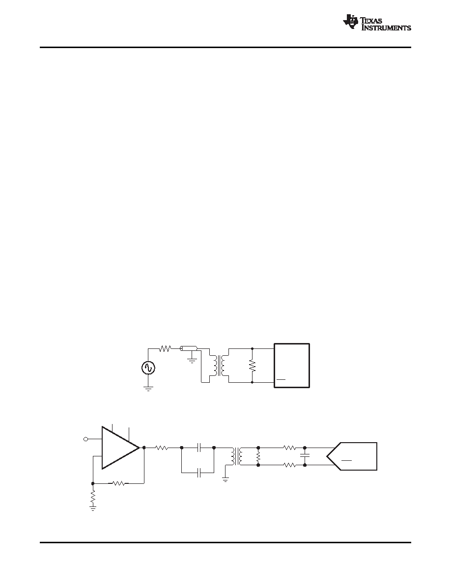
The ADS5424 obtains optimum performance when the analog inputs are driven differentially. The circuit in
Figure 17 shows one possible configuration using an RF transformer with termination either on the primary or on
the secondary of the transformer. If voltage gain is required, a step-up transformer can be used. For higher gains
that would require impractical higher turn ratios on the transformer, a single-ended amplifier driving the
transformer can be used (see Figure 18). Another circuit optimized for performance would be the one on
Figure 19, using the THS4304 or the OPA695. Texas Instruments has shown excellent performance on this
configuration up to 10-dB gain with the THS4304 and at 14-dB gain with the OPA695. For the best performance,
they need to be configured differentially after the transformer (as shown) or in inverting mode for the OPA695
(see SBAA113); otherwise, HD2 from the op amps limits the useful frequency.
Figure 17. Converting a Single-Ended Input to a Differential Signal Using RF Transformers
Figure 18. Using the OPA695 With the ADS5424
16
Copyright 2008–2009, Texas Instruments Incorporated
Product Folder Link(s): ADS5424-SP
相關(guān)PDF資料 |
PDF描述 |
|---|---|
| 5962-0720701VXC | 1-CH 13-BIT PROPRIETARY METHOD ADC, PARALLEL ACCESS, CQFP84 |
| 5962-0720801VXC | 1-CH 12-BIT PROPRIETARY METHOD ADC, PARALLEL ACCESS, CQFP84 |
| 5962-0724301HXC | 1-OUTPUT 66 W DC-DC REG PWR SUPPLY MODULE |
| 5962-0724305HXC | 1-OUTPUT 100 W DC-DC REG PWR SUPPLY MODULE |
| 5962-0724304HXC | 1-OUTPUT 120 W DC-DC REG PWR SUPPLY MODULE |
相關(guān)代理商/技術(shù)參數(shù) |
參數(shù)描述 |
|---|---|
| 5962-0720701VXC | 制造商:TI 制造商全稱:Texas Instruments 功能描述:CLASS V, 13 BIT, 250 MSPS ANALOG-TO-DIGITAL CONVERTER |
| 5962-0720801VXC | 制造商:Texas Instruments 功能描述:ADS5463MHFG-V - Rail/Tube |
| 5962-0721201QXC | 制造商:INTERSIL 制造商全稱:Intersil Corporation 功能描述:Video Distribution Amplifier |
| 5962-0721301QHC | 制造商:INTERSIL 制造商全稱:Intersil Corporation 功能描述:500MHz Rail-to-Rail Amplifiers |
| 5962-0721301QXC | 制造商:INTERSIL 制造商全稱:Intersil Corporation 功能描述:500MHz Rail-to-Rail Amplifiers |
發(fā)布緊急采購(gòu),3分鐘左右您將得到回復(fù)。