- 您現(xiàn)在的位置:買賣IC網(wǎng) > PDF目錄358638 > 3D7444-1.5 (DATA DELAY DEVICES INC) MONOLITHIC QUAD 4-BIT PROGRAMMABLE DELAY LINE (SERIES 3D7444) PDF資料下載
參數(shù)資料
| 型號(hào): | 3D7444-1.5 |
| 廠商: | DATA DELAY DEVICES INC |
| 元件分類: | 通用總線功能 |
| 英文描述: | MONOLITHIC QUAD 4-BIT PROGRAMMABLE DELAY LINE (SERIES 3D7444) |
| 中文描述: | SILICON DELAY LINE, TRUE OUTPUT, PDIP14 |
| 封裝: | DIP-14 |
| 文件頁(yè)數(shù): | 3/6頁(yè) |
| 文件大小: | 157K |
| 代理商: | 3D7444-1.5 |
3D7444
POWER SUPPLY AND
TEMPERATURE CONSIDERATIONS
The delay of CMOS integrated circuits is strongly
dependent on power supply and temperature.
The monolithic 3D7444 programmable delay line
utilizes novel and innovative compensation
circuitry to minimize the delay variations induced
by fluctuations in power supply and/or
temperature.
The
thermal coefficient
is reduced to
400
PPM/C
, which is equivalent to a variation, over
the 0C-70 C operating range, of
±
2%
from the
room-temperature delay settings. The
power
supply coefficient
is reduced, over the 4.75V-
5.25V operating range, to
±
1.5%
of the delay
settings at the nominal 5VDC power supply
and/or
±
2ns
, whichever is greater.
It is essential that the power supply pin be
adequately bypassed and filtered. In addition,
the power bus should be of as low an
impedance construction as possible. Power
planes are preferred.
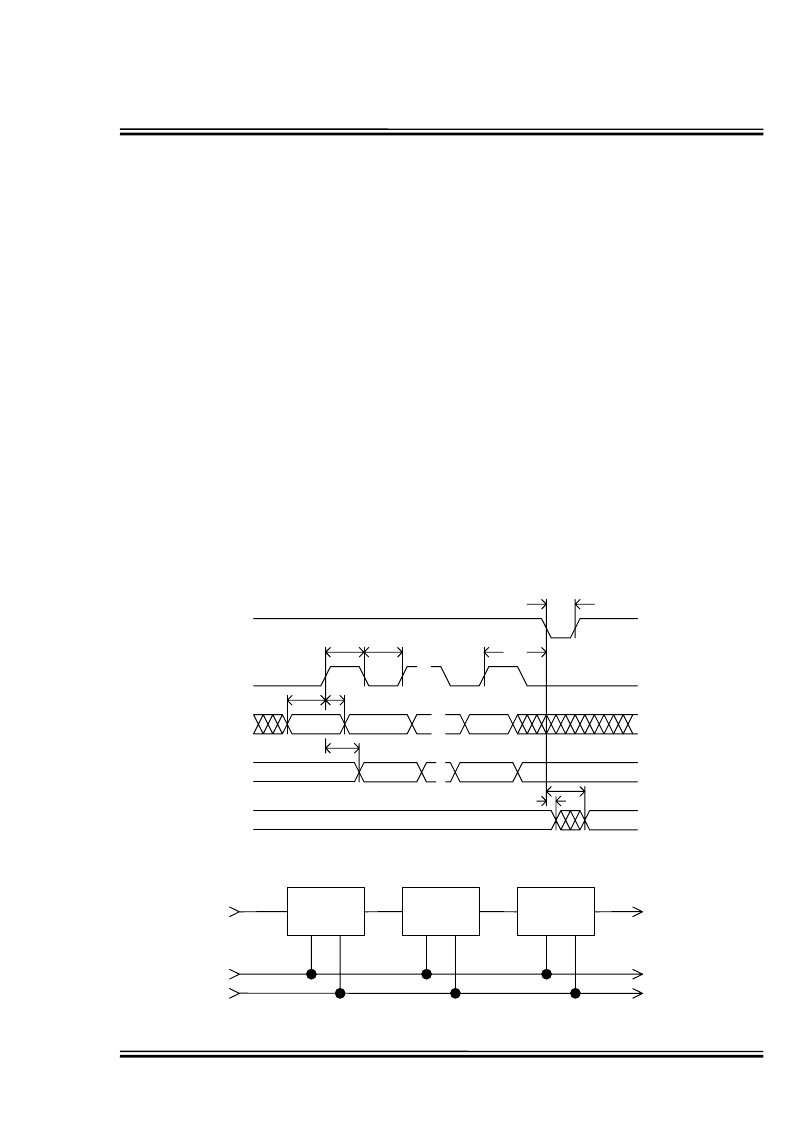
PROGRAMMED DELAY (ADDRESS)
UPDATE
A delay line is a memory device. It stores
information present at the input for a time equal
to the delay setting before presenting it at the
output with minimal distortion. Each 4-bit delay
line in the 3D7444 can be represented by 15
serially connected delay elements (individually
addressed by the programming data), each
capable of storing data for a time equal to the
device increment (step time). The delay line
memory property, in conjunction with the
operational requirement of “instantaneously”
connecting the delay element addressed by the
programming data to the output, may inject
spurious information onto the output data stream.
In order to ensure that spurious outputs do not
occur, it is essential that the input signal be idle
(held high or low) for a short duration prior to
updating the programmed delay. This duration is
given by the maximum programmable delay.
Satisfying this requirement allows the delay line
to “clear” itself of spurious edges. When the new
address is loaded, the input signal can begin to
switch (and the new delay will be valid) after a
time given by
t
PDV
or
t
EDV
(see section below).
NEW
VALUES
NEW
BIT 1
NEW
BIT 20
NEW
BIT 2
t
PCQ
OLD
BIT 1
OLD
BIT 2
OLD
BIT 20
LATCH
(AL)
CLOCK
(SC)
SERIAL
INPUT
(SI)
SERIAL
OUTPUT
(SO)
DELAY
TIMES
t
LW
t
CW
t
CW
t
CSL
t
DSC
t
DHC
t
LDV
t
LDX
PREVIOUS VALUES
Figure 2: Serial interface timing diagram
NEW
BIT 1
FROM
WRITING
DEVICE
TO
NEXT
DEVICE
SI
SO
SC
AL
3D7444
3D7444
SI
3D7444
SI
Figure 3: Cascading Multiple Devices
SO
SC
AL
SO
SC
AL
Doc #03006
12/8/03
DATA DELAY DEVICES, INC.
3 Mt. Prospect Ave. Clifton, NJ 07013
3
相關(guān)PDF資料 |
PDF描述 |
|---|---|
| 3D7501Z | MONOLITHIC MANCHESTER ENCODER |
| 3D7501 | MONOLITHIC MANCHESTER ENCODER |
| 3D7501D | MONOLITHIC MANCHESTER ENCODER |
| 3D7501G | MONOLITHIC MANCHESTER ENCODER |
| 3D7501H | MONOLITHIC MANCHESTER ENCODER |
相關(guān)代理商/技術(shù)參數(shù) |
參數(shù)描述 |
|---|---|
| 3D7444-2 | 制造商:DATADELAY 制造商全稱:Data Delay Devices, Inc. 功能描述:MONOLITHIC QUAD 4-BIT PROGRAMMABLE DELAY LINE (SERIES 3D7444) |
| 3D7444-20 | 制造商:DATADELAY 制造商全稱:Data Delay Devices, Inc. 功能描述:MONOLITHIC QUAD 4-BIT PROGRAMMABLE DELAY LINE (SERIES 3D7444) |
| 3D7444-25 | 制造商:DATADELAY 制造商全稱:Data Delay Devices, Inc. 功能描述:MONOLITHIC QUAD 4-BIT PROGRAMMABLE DELAY LINE (SERIES 3D7444) |
| 3D7444-4 | 制造商:DATADELAY 制造商全稱:Data Delay Devices, Inc. 功能描述:MONOLITHIC QUAD 4-BIT PROGRAMMABLE DELAY LINE (SERIES 3D7444) |
| 3D7444-5 | 制造商:DATADELAY 制造商全稱:Data Delay Devices, Inc. 功能描述:MONOLITHIC QUAD 4-BIT PROGRAMMABLE DELAY LINE (SERIES 3D7444) |
發(fā)布緊急采購(gòu),3分鐘左右您將得到回復(fù)。