- 您現(xiàn)在的位置:買賣IC網(wǎng) > PDF目錄371395 > 24C44 256-Bit Serial Nonvolatile CMOS Static RAM PDF資料下載
參數(shù)資料
| 型號(hào): | 24C44 |
| 英文描述: | 256-Bit Serial Nonvolatile CMOS Static RAM |
| 中文描述: | 256位串行非易失性的CMOS靜態(tài)RAM |
| 文件頁數(shù): | 5/8頁 |
| 文件大?。?/td> | 44K |
| 代理商: | 24C44 |

CAT24C44
5
Doc. No. 25019-0A 2/98 N-1
DEVICE OPERATION
The CAT24C44 is intended for use with standard micro-
processors. The CAT24C44 is organized as 16 registers
by 16 bits. Seven 8-bit instructions control the device’s
operating modes, the RAM reading and writing, and the
E
2
PROM storing and recalling. It is also possible to
control the E
2
PROM store and recall functions in hard-
ware with the
STORE
and
RECALL
pins. The CAT24C44
operates on a single 5V supply and will generate, on
chip, the high voltage required during a RAM to E
2
PROM
storing operation.
Instructions, addresses and write data are clocked into
the DI pin on the rising edge of the clock (SK). The DO
pin remains in a high impedance state except when
outputting data from the device. The
CE
(Chip Enable)
pin must remain high during the entire data transfer.
The format for all instructions sent to the CAT24C44 is
a logical ‘1’ start bit, 4 address bits (data read or write
operations) or 4 “Don’t Care” bits (device mode opera-
tions), and a 3-bit op code (see Instruction Set). For data
write operations, the 8-bit instruction is followed by 16
bits of data. For data read instructions, DO will come out
of the high impedance state and enable 16 bits of data
to be clocked from the device. The 8th bit of the read
instruction is a “Don’t Care” bit. This is to eliminate any
bus contention that would occur in applications where
the DI and DO pins are tied together to form a common
DI/DO line. A word of caution while clocking data to and
from the device: If the
CE
pin is prematurely deselected
while shifting in an instruction, that instruction will not be
executed, and the shift register internal to the CAT24C44
will be cleared. If there are more than or less than 16
clocks during a memory data transfer, an improper data
transfer will result. The SK clock is completely static
allowing the user to stop the clock and restart it to
resume shifting of data.
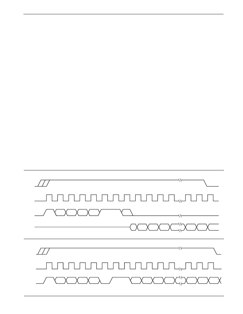
Read
Upon receiving a start bit, 4 address bits, and the 3-bit
read command (clocked into the DI pin), the DO pin of
the CAT24C44 will come out of the high impedance state
and the 16 bits of data, located at the address specified
in the instructions, will be clocked out of the device.
When clocking data from the device, the first bit clocked
out (DO) is timed from the falling edge of the 8th clock,
all succeeding bits (D1–D15) are timed from the rising
edge of the clock.
Write
After receiving a start bit, 4 address bits, and the 3-bit
WRITE command, the 16-bit word is clocked into the
device for storage into the RAM memory location speci-
fied. The
CE
pin must remain high during the entire write
operation.
Figure 1. RAM Read Cycle Timing
5157 FHD F02
Note:
(1) Bit 8 of READ instruction is “Don’t Care”.
Figure 2. RAM Write Cycle Timing
5157 FHD F03
SK
CE
DI
D0
1
2
3
4
5
6
7
8
9
10
11
12
22
23
24
1
D1
D2
D3
D13
D14
D15
A
1
1
A
A
A
0
SK
CE
DI
DO
HIGH-Z
D0
1
2
3
4
5
6
7
8
9
10
11
12
22
23
24
1
D1
D2
D3
D14
D15
D0
A
X
1
1
A
A
A
(8)
(1)
相關(guān)PDF資料 |
PDF描述 |
|---|---|
| 24C512 | 2-wire Serial EEPROM |
| 24C65 | 64K 5.0V I 2 C Smart Serial EEPROM |
| 24C65-EP | 64K 5.0V I 2 C Smart Serial EEPROM |
| 24C65-ESM | 64K 5.0V I 2 C Smart Serial EEPROM |
| 24C65-IP | 64K 5.0V I 2 C Smart Serial EEPROM |
相關(guān)代理商/技術(shù)參數(shù) |
參數(shù)描述 |
|---|---|
| 24C48D | 制造商:未知廠家 制造商全稱:未知廠家 功能描述:Analog IC |
| 24C48S | 制造商:未知廠家 制造商全稱:未知廠家 功能描述:Analog IC |
| 24C4PH003F-A174 | 制造商: 功能描述: 制造商:undefined 功能描述: |
| 24C512 | 制造商:ATMEL 制造商全稱:ATMEL Corporation 功能描述:2-wire Serial EEPROM |
| 24C512-10TI-2.7 | 制造商: 功能描述: 制造商:undefined 功能描述: |
發(fā)布緊急采購,3分鐘左右您將得到回復(fù)。