- 您現(xiàn)在的位置:買賣IC網(wǎng) > PDF目錄222090 > 13715-806-XTD (ON SEMICONDUCTOR) 300 MHz, OTHER CLOCK GENERATOR, PDSO16 PDF資料下載
參數(shù)資料
| 型號(hào): | 13715-806-XTD |
| 廠商: | ON SEMICONDUCTOR |
| 元件分類: | 時(shí)鐘產(chǎn)生/分配 |
| 英文描述: | 300 MHz, OTHER CLOCK GENERATOR, PDSO16 |
| 封裝: | 0.150 INCH, GREEN, SOIC-16 |
| 文件頁數(shù): | 8/19頁 |
| 文件大小: | 582K |
| 代理商: | 13715-806-XTD |
FS714x Programmable Phase-Locked Loop Clock Generator
Data Sheet
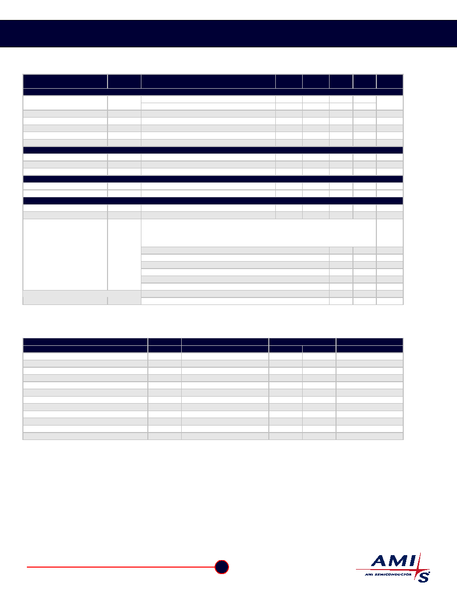
Table 13: AC Timing Specifications
Parameter
Symbol
Conditions/Description
Clock
(MHz)
Min.
Typ.
Max.
Units
Overall
CMOS outputs
0
150
Output frequency*
fo(max)
PECL outputs
0
300
MHz
VCO frequency*
fVCO
40
400
MHz
CMOS mode rise time*
tr
CL = 7pF
1
ns
CMOS mode fall time*
tf
CL = 7pF
1
ns
PECL mode rise time*
tr
CL = 7pF; RL = 65 ohm
1
ns
PECL mode fall time*
tf
CL = 7pF; RL = 65 ohm
1
ns
Reference Frequency Input (REF)
Input frequency
FREF
80
MHz
Reference high time
tREHF
3
ns
Reference low time
tREFL
3
ns
Sync Control Input (SYNC)
Sync high time
tSYNCH
For orderly CLK stop/start
3
TCLK
Sync low time
tSYNCL
For orderly CLK stop/start
3
TCLK
Clock Output (CLKP, CLKN)
Duty cycle (CMOS mode)*
Measured at 1.4V
50
%
Duty cycle (PECL mode)*
Measured at zero crossings of (VCLKP – VCLKN)
50
%
For valid programming solutions. Long-term (or cumulative) jitter specified is RMS
position error of any edge compared with an ideal clock generated from the same
reference frequency. It is measured with a time interval analyzer using a 500
microsecond window, using statistics gathered over 1000 samples.
ps
FREF/NREF > 1000kHz
25
ps
FREF/NREF ~= 500kHz
50
ps
FREF/NREF ~= 250kHz
100
ps
FREF/NREF ~= 125kHz
190
ps
FREF/NREF ~= 62.5kHz
240
ps
Jitter, long term (
σy(τ))*
tj(LT)
FREF/NREF ~= 31.5kHz
300
ps
40MHz < VCO frequency <100MHz
75
ps
Jitter, period (peak-peak)*
tj(ΔP)
VCO frequency > 100MHz
50
ps
Unless otherwise stated, VDD = 3.3V ± 10%, no load on any output, and ambient temperature range TA = 0°C to 70°C. Parameters denoted with an asterisk (*) represent
nominal characterization data and are not production tested to any specific limits. MIN and MAX characterization data are ± 3
σ from typical.
Table 14: Serial Interface Timing Specifications
Parameter
Symbol
Conditions/Description
Fast Mode
Units
Min.
Max.
Clock frequency
fSCL
SCL
0
400
kHz
Bus free time between STOP and START
tBUF
1300
ns
Set-up time, START (repeated)
Tsu:STA
600
ns
Hold time, START
thd:STA
600
ns
Set-up time, data input
Tsu:DAT
SDA
100
ns
Hold time, data input
thd:DAT
SDA
0
ns
Output data valid from clock
tAA
900
ns
Rise time, data and clock
tR
SDA, SCL
300
ns
Fall time, data and clock
tF
SDA, SCL
300
ns
High time, clock
tHI
SCL
600
ns
Low time, clock
tLO
SCL
1300
ns
Set-up time, STOP
Tsu:STO
600
ns
Unless otherwise stated, VDD = 3.3V ± 10%, no load on any output, and ambient temperature range TA = 0°C to 70°C. Parameters denoted with an asterisk (*) represent
nominal characterization data and are not production tested to any specific limits. MIN and MAX characterization data are ± 3
σ from typical.
16
AMI Semiconductor – Dec, 2007 – Rev. 4.0
www.amis.com
Specifications subject to change without notice
相關(guān)PDF資料 |
PDF描述 |
|---|---|
| 1374610-3 | INTERCONNECTION DEVICE |
| 1376137-1 | POWER CONNECTOR |
| 1380B-8 | BRASS, GOLD FINISH, PCB TERMINAL |
| 1390D-17 | BRASS, PCB TERMINAL |
| 1390D-1 | BRASS, SILVER FINISH, PCB TERMINAL |
相關(guān)代理商/技術(shù)參數(shù) |
參數(shù)描述 |
|---|---|
| 13716 | 功能描述:TOOL SET NUT DRVR PREC 6PC RoHS:否 類別:工具 >> 螺釘和螺母驅(qū)動(dòng)器 - 裝置 系列:- 標(biāo)準(zhǔn)包裝:1 系列:* 其它名稱:Q4953585A |
| 13-716 | 制造商:3M 制造商全稱:3M Electronics 功能描述:Specialty Terminals |
| 1371640000 | 功能描述:TBY-C3-UNIV-SP-2KS-S 制造商:weidmuller 系列:* 零件狀態(tài):在售 標(biāo)準(zhǔn)包裝:1 |
| 13716403 | 功能描述:汽車連接器 TERM DSQ 280 F.SN3 FEM ASY RoHS:否 制造商:Amphenol SINE Systems 產(chǎn)品:Contacts 系列:ATP 位置數(shù)量: 型式:Female 安裝風(fēng)格: 端接類型: 觸點(diǎn)電鍍:Nickel |
| 13716-50-0-4/3V | 制造商:HUBER+SUHNER 功能描述:RF COAXIAL PANEL MOUNT CONNECTOR |
發(fā)布緊急采購,3分鐘左右您將得到回復(fù)。