- 您現(xiàn)在的位置:買賣IC網(wǎng) > PDF目錄373786 > ZL50233GD (Zarlink Semiconductor Inc.) 4 Channel Voice Echo Cancellor PDF資料下載
參數(shù)資料
| 型號(hào): | ZL50233GD |
| 廠商: | Zarlink Semiconductor Inc. |
| 英文描述: | 4 Channel Voice Echo Cancellor |
| 中文描述: | 4通道語音回聲消除器 |
| 文件頁數(shù): | 20/37頁 |
| 文件大小: | 625K |
| 代理商: | ZL50233GD |
第1頁第2頁第3頁第4頁第5頁第6頁第7頁第8頁第9頁第10頁第11頁第12頁第13頁第14頁第15頁第16頁第17頁第18頁第19頁當(dāng)前第20頁第21頁第22頁第23頁第24頁第25頁第26頁第27頁第28頁第29頁第30頁第31頁第32頁第33頁第34頁第35頁第36頁第37頁
ZL50233
Data Sheet
20
Zarlink Semiconductor Inc.
Note: In order to correctly write to Control Register 1 and 2 of ECB, it is necessary to write the data twice to the register, one
immediately after another. The two writes must be separated by at least 350ns and no more than 20us.
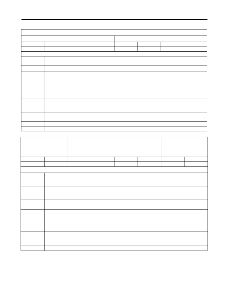
Echo Canceller B (ECB): Control Register 1
Power-up 02
hex
Bit 6
INJDis
R/W Address: 20
hex
+ Base Address
Bit 3
Bit 2
Bypass
AdpDis
Bit 7
Reset
Bit 5
BBM
Bit 4
PAD
Bit 1
1
Bit 0
0
Functional Description of Register Bits
When high, the power-up initialization is executed which presets all register bits including this bit
and clears the Adaptive Filter coefficients.
When high, the noise injection process is disabled. When low, noise injection is enabled.
Reset
INJDis
BBM
When high, the Back to Back configuration is enabled. When low, the Normal configuration is
enabled. Note: Do not enable Extended-Delay and BBM configurations at the same time. Always
set
both
BBM bits of the two echo cancellers (Control Register 1) of the same group to the same
logic value to avoid conflict.
PAD
When high, 12dB of attenuation is inserted into the Rin to Rout path. When low, the Gains register
controls the signal levels.
When high, Sin data is by-passed to Sout and Rin data is by-passed to Rout. The Adaptive Filter
coefficients are set to zero and the filter adaptation is stopped. When low, output data on both
Sout and Rout is a function of the echo canceller algorithm.
When high, echo canceller adaptation is disabled. The Voice Processor cancels echo.
When low, the echo canceller dynamically adapts to the echo path characteristics.
Bits marked as “1” or “0” are reserved bits and should be written as indicated.
Control Register 1 (Echo Canceller B) Bit 0 is a reserved bit and should be written “0”.
Bypass
AdpDis
1
0
Power-up
00
hex
ECA: Control Register 2
R/W Address:
01
hex
+ Base Address
R/W Address:
21
hex
+ Base Address
Bit 1
MuteS
ECB: Control Register 2
Bit 7
TDis
Bit 6
PHDis
Bit 5
NLPDis
Bit 4
AutoTD
Bit 3
NBDis
Bit 2
HPFDis
Bit 0
MuteR
Functional Description of Register Bits
When high, tone detection is disabled. When low, tone detection is enabled. When both Echo
Cancellers A and B TDis bits are high, Tone Disable processors are disabled entirely and are put
into Power Down mode.
When high, the tone detectors will trigger upon the presence of a 2100 Hz tone regardless of the
presence/absence of periodic phase reversals. When low, the tone detectors will trigger only upon
the presence of a 2100 Hz tone with periodic phase reversals.
When high, the non-linear processor is disabled. When low, the non-linear processors function
normally. Useful for G.165 conformance testing.
TDis
PHDis
NLPDis
AutoTD
When high, the echo canceller puts itself in Bypass mode when the tone detectors detect the
presence of 2100 Hz tone. See PHDis for qualification of 2100 Hz tones.
When low, the echo canceller algorithm will remain operational regardless of the state of the 2100
Hz tone detectors.
When high, the narrow-band detector is disabled. When low, the narrow-band detector is enabled.
When high, the offset nulling high pass filters are bypassed in the Rin and Sin paths. When low,
the offset nulling filters are active and will remove DC offsets on PCM input signals.
When high, data on Sout is muted to quiet code. When low, Sout carries active code.
When high, data on Rout is muted to quiet code. When low, Rout carries active code.
NBDis
HPFDis
MuteS
MuteR
相關(guān)PDF資料 |
PDF描述 |
|---|---|
| ZL50233GDC | 4 Channel Voice Echo Cancellor |
| ZL50233QC | 4 Channel Voice Echo Cancellor |
| ZL50233QCC | 4 Channel Voice Echo Cancellor |
| ZL50233 | 4 Channel Voice Echo Cancellor |
| ZL50234 | SHOCKSAFE FUSEHOLDER W/ COVER |
相關(guān)代理商/技術(shù)參數(shù) |
參數(shù)描述 |
|---|---|
| ZL50233GDC | 制造商:ZARLINK 制造商全稱:Zarlink Semiconductor Inc 功能描述:4 Channel Voice Echo Cancellor |
| ZL50233GDG | 制造商:Microsemi Corporation 功能描述:ECHO CANCELLER CHIP 4-CH G.165/G.168/G.711 W/ TONE DETECTION - Trays 制造商:MICROSEMI CONSUMER MEDICAL PRODUCT GROUP 功能描述:IC VOICE ECHO CANCEL 4CH 208LBGA 制造商:Microsemi Corporation 功能描述:IC VOICE ECHO CANCEL 4CH 208LBGA |
| ZL50233QC | 制造商:ZARLINK 制造商全稱:Zarlink Semiconductor Inc 功能描述:4 Channel Voice Echo Cancellor |
| ZL50233QCC | 制造商:ZARLINK 制造商全稱:Zarlink Semiconductor Inc 功能描述:4 Channel Voice Echo Cancellor |
| ZL50233QCG1 | 制造商:Microsemi Corporation 功能描述:ECHO CANCELLER CHIP 4-CH G.165/G.168/G.711 W/ TONE DETECTION - Trays 制造商:MICROSEMI CONSUMER MEDICAL PRODUCT GROUP 功能描述:IC VOICE ECHO CANCEL 4CH 100LQFP 制造商:Microsemi Corporation 功能描述:IC VOICE ECHO CANCEL 4CH 100LQFP |
發(fā)布緊急采購,3分鐘左右您將得到回復(fù)。