- 您現(xiàn)在的位置:買賣IC網(wǎng) > PDF目錄373782 > ZL20200LDG1 (Zarlink Semiconductor Inc.) Dual Band IS136/AMPS Transceiver PDF資料下載
參數(shù)資料
| 型號(hào): | ZL20200LDG1 |
| 廠商: | Zarlink Semiconductor Inc. |
| 英文描述: | Dual Band IS136/AMPS Transceiver |
| 中文描述: | 雙頻IS136/AMPS收發(fā)器 |
| 文件頁數(shù): | 9/51頁 |
| 文件大小: | 485K |
| 代理商: | ZL20200LDG1 |
第1頁第2頁第3頁第4頁第5頁第6頁第7頁第8頁當(dāng)前第9頁第10頁第11頁第12頁第13頁第14頁第15頁第16頁第17頁第18頁第19頁第20頁第21頁第22頁第23頁第24頁第25頁第26頁第27頁第28頁第29頁第30頁第31頁第32頁第33頁第34頁第35頁第36頁第37頁第38頁第39頁第40頁第41頁第42頁第43頁第44頁第45頁第46頁第47頁第48頁第49頁第50頁第51頁
ZL20200
Data Sheet
9
Zarlink Semiconductor Inc.
1.1 Receive Path
The IF input receives an input signal from IS136/AMPS filter. The differential input stage is followed by an agc
amplifier. Gain control is provided from an external analog voltage. After the agc amplifier the signal is then down-
converted to a low IF frequency and the signal flow then depends on the mode selected. All internal signals are
differential. The LO frequency for the down conversion is derived from an on chip oscillator and PLL. The LO
frequency can be programmed to be either oscillator frequency divided by 2 or 4. When in divide by 2 mode a DLL
(Delay Locked Loop) circuit can be selected to maintain accurate quadrature. It is particularly important to have
good quadrature in IS136/AMPS modes using a low IF frequency, to achieve the required image rejection in
conjunction with the following polyphase bandpass filter. It is also possible to programme high side or low LO
injection. Each receive mode will now be described in more detail
1.1.1 IS136
The IS136 receive signal path is shown in detail in Figure 4 and performance for each stage is summarized in the
following table.
The output of the agc amplifier is down-converted using a quadrature mixer to a low IF of 60 kHz. High side or low
side LO injection can be selected. The In Phase (I) and Quadrature (Q) signals at 60 kHz are then passed through
anti alias filter stage to remove any high frequency signals prior to subsequent sampling. The 60 kHz IF signals are
then fed into a switched capacitor polyphase bandpass filter which not only provides filtering but also provides
image rejection. This switched capacitor filter provides very stable performance and no calibration is required. After
the bandpass filter the 60 kHz IF signal is further amplified and then mixed down to baseband I and Q signals.
Additional filtering is required at baseband to remove spurii from the down-converter. This filtering is provide in two
stages, the first stage is a switched capacitor filter with the second stage being a smoothing filter to remove clock
breakthrough from the preceding switched capacitor filter. The differential baseband outputs can then be fed
directly into analog to digital converters on a baseband processor.
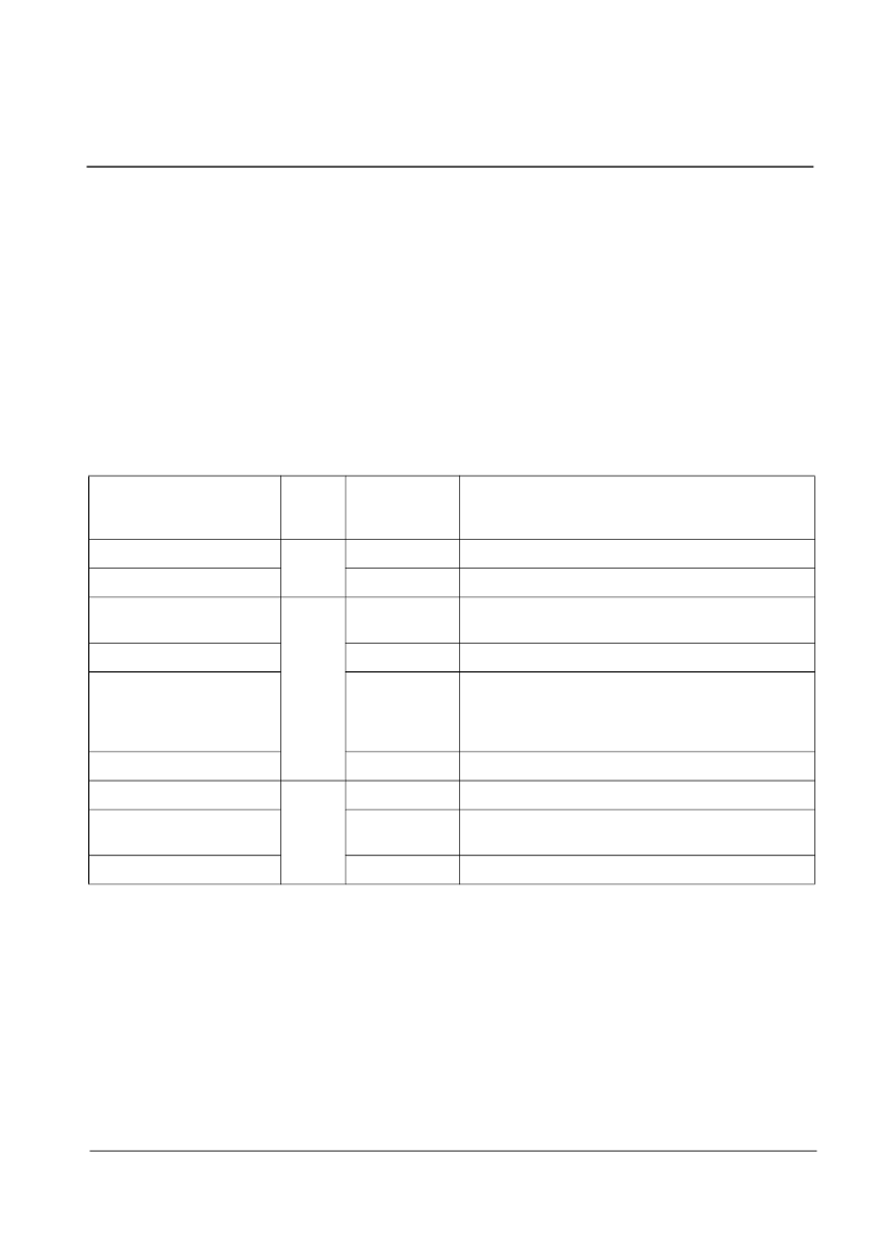
Circuit
Block
Gain
(dB)
Filter
Bandwidth
(If Applicable)
Description
IF Input (IF1)
26
max
Differential IF input stage
AGC Amplifier
AGC Amplifier - Gain control range 90 dB
Quadrature
Down-converter
47
Down-conversion to 60 kHz IF
Anti-alias filter
230 kHz
Low pass Butterworth (n= 3)
Band Pass Filter
+/- 20 kHz
Switched capacitor polyphase Chebyshev. Also
provides typically 30 dB image rejection. Centre
frequency = 60 kHz. Clock frequencies 1.44 MHz and
720 kHz.
Gain Stage
Baseband Down-converter
7
Down conversion to baseband I and Q signals
Baseband filter 1
37.5 kHz
Switched capacitor low pass Chebyshev. Clock
frequency = 240 kHz
Baseband filter 2
60 kHz
Smoothing filter. Low pass Butterworth
Table 1 - IS136 Receive Gain and Filter Distribution
相關(guān)PDF資料 |
PDF描述 |
|---|---|
| ZL20200 | Dual Band IS136/AMPS Transceiver |
| ZL20200LCE | Dual Band IS136/AMPS Transceiver |
| ZL20200LCF | Dual Band IS136/AMPS Transceiver |
| ZL20200LDE | Dual Band IS136/AMPS Transceiver |
| ZL20250 | 2.5G Multimode Transceiver |
相關(guān)代理商/技術(shù)參數(shù) |
參數(shù)描述 |
|---|---|
| ZL20250 | 制造商:ZARLINK 制造商全稱:Zarlink Semiconductor Inc 功能描述:2.5G Multimode Transceiver |
| ZL20250/LCE | 制造商:Microsemi Corporation 功能描述:RF TRNSCVR FM 56QFN - Bulk |
| ZL20250/LCF | 制造商:Microsemi Corporation 功能描述:RF TRNSCVR FM 56QFN - Bulk |
| ZL20250LCE | 制造商:ZARLINK 制造商全稱:Zarlink Semiconductor Inc 功能描述:2.5G Multimode Transceiver |
| ZL20250LCF | 制造商:ZARLINK 制造商全稱:Zarlink Semiconductor Inc 功能描述:2.5G Multimode Transceiver |
發(fā)布緊急采購,3分鐘左右您將得到回復(fù)。