- 您現(xiàn)在的位置:買賣IC網(wǎng) > PDF目錄373771 > Z8S180 (ZiLOG, Inc.) CAP 0.1UF 100V +80-20% Z5U AXIAL TR-14 PDF資料下載
參數(shù)資料
| 型號: | Z8S180 |
| 廠商: | ZiLOG, Inc. |
| 英文描述: | CAP 0.1UF 100V +80-20% Z5U AXIAL TR-14 |
| 中文描述: | 強(qiáng)化Z180微處理器 |
| 文件頁數(shù): | 39/70頁 |
| 文件大小: | 387K |
| 代理商: | Z8S180 |
第1頁第2頁第3頁第4頁第5頁第6頁第7頁第8頁第9頁第10頁第11頁第12頁第13頁第14頁第15頁第16頁第17頁第18頁第19頁第20頁第21頁第22頁第23頁第24頁第25頁第26頁第27頁第28頁第29頁第30頁第31頁第32頁第33頁第34頁第35頁第36頁第37頁第38頁當(dāng)前第39頁第40頁第41頁第42頁第43頁第44頁第45頁第46頁第47頁第48頁第49頁第50頁第51頁第52頁第53頁第54頁第55頁第56頁第57頁第58頁第59頁第60頁第61頁第62頁第63頁第64頁第65頁第66頁第67頁第68頁第69頁第70頁
Z80180/Z8S180/Z8L180
Enhanced Z180 Microprocessor
Zilog
DS971800401
P R E L I M I N A R Y
1-39
1
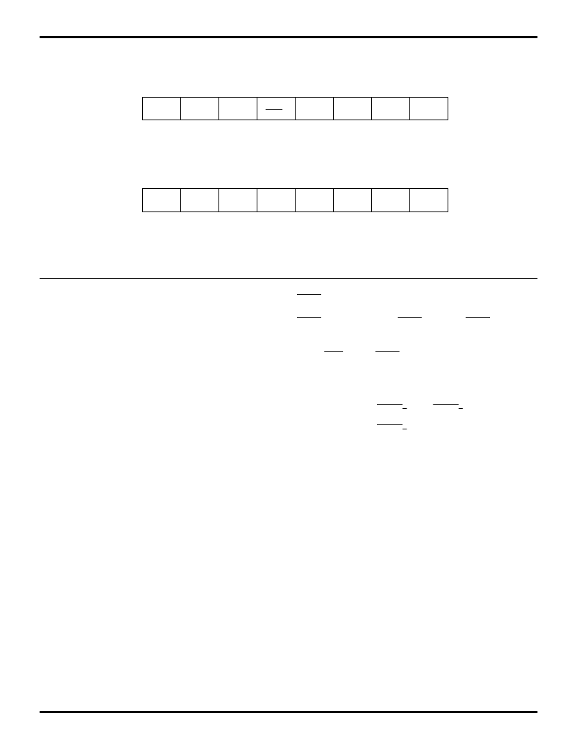
ASCI CHANNEL CONTROL REGISTER A
MPE: Multi-Processor Mode Enable (bit 7).
The ASCI
has a multiprocessor communication mode that utilizes an
extra data bit for selective communication when a number
of processors share a common serial bus. Multiprocessor
data format is selected when the MP bit in CNTLB is set to
1. If multiprocessor mode is not selected (MP bit in CNTLB
= 0), MPE has no effect. If multiprocessor mode is select-
ed, MPE enables or disables the “wake-up” feature as fol-
lows. If MBE is set to 1, only received bytes in which the
MPB (multiprocessor bit) = 1 can affect the RDRF and er-
ror flags. Effectively, other bytes (with MPB = 0) are “ig-
nored” by the ASCI. If MPE is reset to 0, all bytes, regard-
less of the state of the MPB data bit, affect the REDR and
error flags. MPE is cleared to 0 during RESET.
RE: Receiver Enable (bit 6).
When RE is set to 1, the
ASCI transmitter is enabled. When TE is reset to 0, the
transmitter is disables and any transmit operation in
progress is interrupted. However, the TDRE flag is not re-
set and the previous contents of TDRE are held. TE is
cleared to 0 in IOSTOP mode during RESET.
TE: Transmitter Enable (bit 5)
. When TE is set to 1, the
ASCI receiver is enabled. When TE is reset to 0, the trans-
mitter is disabled and any transmit operation in progress is
interrupted. However, the TDRE flag is not reset and the
previous contents of TDRE are held. TE is cleared to 0 in
IOSTOP mode during RESET.
RTS0: Request to Send Channel 0 (bit 4 in CNTLA0
only).
If bit 4 of the System Configuration Register is 0, the
RTS0/TxS pin has the RTS0 function. RTS0 allows the
ASCI to control (start/stop) another communication devic-
es transmission (for example, by connecting to that de-
vice’s CTS input). RTS0 is essentially a 1 bit output port,
having no side effects on other ASCI registers or flags.
Bit 4 in CNTLA1 is used.
CKA1D = 1, CKA1/TEND
0
pin = TEND
0
CKA1D = 0, CKA1/TEND
0
pin = CKA1
Cleared to 0 on reset.
MPBR/EFR: Multiprocessor Bit Receive/Error Flag Re-
set (bit 3).
When multiprocessor mode is enabled (MP in
CNTLB = 1), MPBR, when read, contains the value of the
MPB bit for the last receive operation. When written to 0,
the EFR function is selected to reset all error flags (OVRN,
FE, PE and BRK in the ASEXT Register) to 0. MPBR/EFR
is undefined during RESET.
Figure 33. ASCI Channel Control Register A
Bit
MPE
RE
R/W
R/W
R/W
TE
7
6
5
4
3
2
1
0
RTS0
MPBR/
EFR
MOD2
MOD1
MOD0
R/W
R/W
ASCI Control Register A 0 (CNTLA0: I/O Address = 00H)
R/W
R/W
R/W
Bit
MPE
RE
R/W
R/W
R/W
TE
7
6
5
4
3
2
1
0
MOD2
MOD1
MOD0
R/W
R/W
ASCI Control Register A 1 (CNTLA1: I/O Address = 01H)
R/W
R/W
R/W
MPBR/
EFR
CKA1D
相關(guān)PDF資料 |
PDF描述 |
|---|---|
| Z8S18006FEC | CAP 1UF 50V 10% X7R AXIAL TR-14 |
| Z8S18006FSC | CAP 0.47UF 50V 10% X7R AXIAL TR-14 |
| Z8S18006PEC | CAP 0.1UF 50V 2% NP0(C0G) AXIAL TR-14 |
| Z8S18006PSC | CAP 1000PF 100V 5% NP0(C0G) DIP-2 TUBE |
| Z90102 | CAP 560PF 100V 10% X7R AXIAL BULK R-MIL-PRF-39014 |
相關(guān)代理商/技術(shù)參數(shù) |
參數(shù)描述 |
|---|---|
| Z8S18000ZCO | 功能描述:開發(fā)板和工具包 - 其他處理器 Z8S180 App Board RoHS:否 制造商:Freescale Semiconductor 產(chǎn)品:Development Systems 工具用于評估:P3041 核心:e500mc 接口類型:I2C, SPI, USB 工作電源電壓: |
| Z8S18000ZEM | 功能描述:仿真器/模擬器 Z8S180 Emulator Kit RoHS:否 制造商:Blackhawk 產(chǎn)品:System Trace Emulators 工具用于評估:C6000, C5000, C2000, OMAP, DAVINCI, SITARA, TMS470, TMS570, ARM 7/9, ARM Cortex A8/R4/M3 用于:XDS560v2 |
| Z8S18006FEC | 制造商:ZILOG 制造商全稱:ZILOG 功能描述:ENHANCED Z180 MICROPROCESSOR |
| Z8S18006FSC | 制造商:ZILOG 制造商全稱:ZILOG 功能描述:ENHANCED Z180 MICROPROCESSOR |
| Z8S18006PEC | 制造商:ZILOG 制造商全稱:ZILOG 功能描述:ENHANCED Z180 MICROPROCESSOR |
發(fā)布緊急采購,3分鐘左右您將得到回復(fù)。