- 您現(xiàn)在的位置:買賣IC網(wǎng) > PDF目錄372964 > Z86L7208FSC (ZILOG INC) IR MICROCONTROLLER PDF資料下載
參數(shù)資料
| 型號: | Z86L7208FSC |
| 廠商: | ZILOG INC |
| 元件分類: | 微控制器/微處理器 |
| 英文描述: | IR MICROCONTROLLER |
| 中文描述: | 8-BIT, MROM, 8 MHz, MICROCONTROLLER, PQFP44 |
| 封裝: | QFP-44 |
| 文件頁數(shù): | 28/71頁 |
| 文件大小: | 364K |
| 代理商: | Z86L7208FSC |
第1頁第2頁第3頁第4頁第5頁第6頁第7頁第8頁第9頁第10頁第11頁第12頁第13頁第14頁第15頁第16頁第17頁第18頁第19頁第20頁第21頁第22頁第23頁第24頁第25頁第26頁第27頁當前第28頁第29頁第30頁第31頁第32頁第33頁第34頁第35頁第36頁第37頁第38頁第39頁第40頁第41頁第42頁第43頁第44頁第45頁第46頁第47頁第48頁第49頁第50頁第51頁第52頁第53頁第54頁第55頁第56頁第57頁第58頁第59頁第60頁第61頁第62頁第63頁第64頁第65頁第66頁第67頁第68頁第69頁第70頁第71頁
Z86C72/C92/L72/L92
IR Microcontroller
Zilog
6-28
P R E L I M I N A R Y
DS97LVO0900
PIN FUNCTIONS
(Continued)
/RESET
(Input, active Low). Initializes the MCU. Reset is
accomplished either through Power-On, Watch-Dog Tim-
er, Stop-Mode Recovery, Low Voltage detection, or exter-
nal reset. During Power-On Reset and Watch-Dog Timer
Reset, the internally generated reset drives the reset pin
Low for the POR time. Any devices driving the reset line
should be open-drain in order to avoid damage from a pos-
sible conflict during reset conditions. Pull-up is provided in-
ternally. There is no internal condition that will not allow an
external reset to occur.
After the POR time, /RESET is a Schmitt-triggered input.
To avoid asynchronous and noisy reset problems, the
Z86L/CX2 is equipped with a reset filter of four external
clocks (4TpC). If the external reset signal is less than 4TpC
in duration, no reset occurs. On the fifth clock after the re-
set is detected, an internal RST signal is latched and held
for an internal register count of 18 external clocks, or for
the duration of the external reset, whichever is longer.
During the reset cycle, /DS is held active Low while /AS cy-
cles at a rate of TpC/2. Program execution begins at loca-
tion 000CH, 5-10 TpC cycles after the RST is released. For
Power-On Reset, the typical reset output time is 5 ms. The
Z86L/CX2 does not reset WDTMR, SMR, P2M, P2, P3, or
P3M registers on a Stop-Mode Recovery operation.
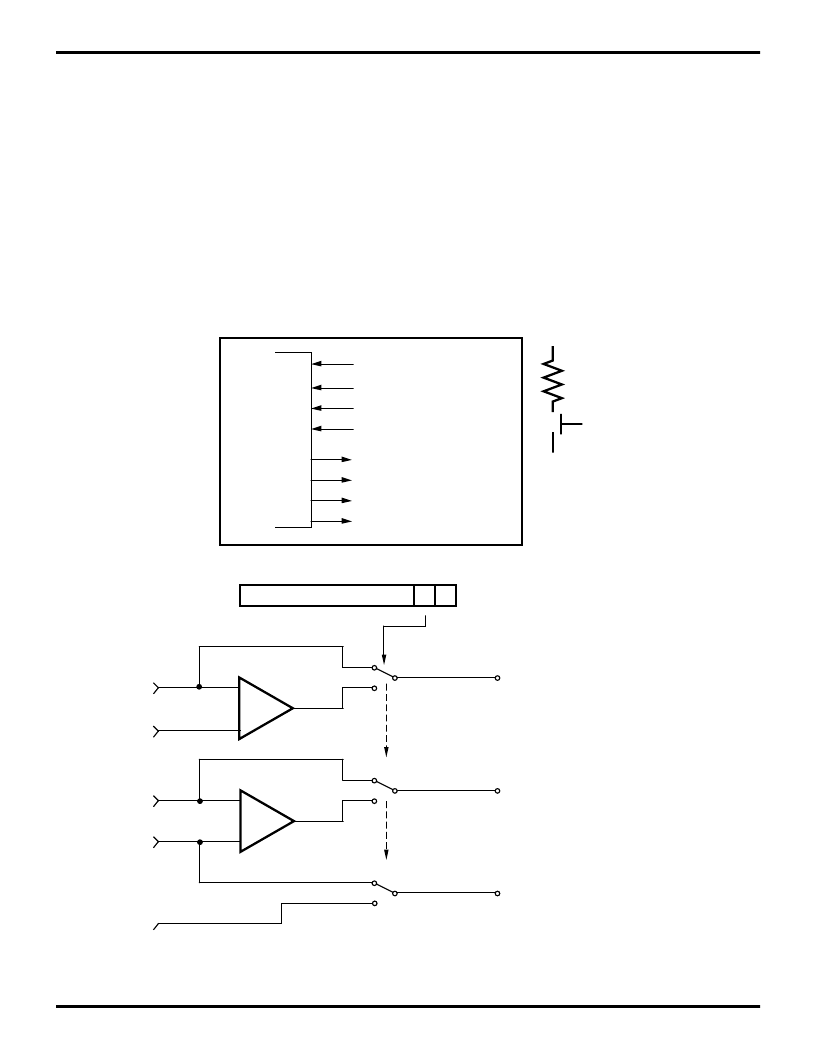
Figure 15. Port 3 Configuration
Port 3
(I/O or Handshake)
Z86L7X
MCU
Pref1
P31
P32
P33
P34
P35
P36
P37
Note:
P31, 32, 33 have a 200 K
mask option.
200 K
Mask
Option
D1
R247 = P3M
P31 (AN1)
P32 (AN2)
P33 (REF2)
From Stop-Mode
Recovery Source of SMR
1 = Analog
0 = Digital
IRQ2, P31 Data Latch
IRQ0, P32 Data Latch
IRQ1, P33 Data Latch
DIG.
AN.
-
+
-
+
Pref1*
Comp1
Comp2
相關(guān)PDF資料 |
PDF描述 |
|---|---|
| Z86L7208PSC | IR MICROCONTROLLER |
| Z86L7208VSC | IR MICROCONTROLLER |
| Z86C7216VSC | IR MICROCONTROLLER |
| Z86C72 | IR MICROCONTROLLER |
| Z86C7216PSC | IR MICROCONTROLLER |
相關(guān)代理商/技術(shù)參數(shù) |
參數(shù)描述 |
|---|---|
| Z86L7208PSC | 制造商:ZILOG 制造商全稱:ZILOG 功能描述:IR MICROCONTROLLER |
| Z86L72-08PSC | 制造商:未知廠家 制造商全稱:未知廠家 功能描述:8-Bit Microcontroller |
| Z86L7208VSC | 制造商:ZILOG 制造商全稱:ZILOG 功能描述:IR MICROCONTROLLER |
| Z86L72-08VSC | 制造商:未知廠家 制造商全稱:未知廠家 功能描述:8-Bit Microcontroller |
| Z86L73 | 制造商:ZILOG 制造商全稱:ZILOG 功能描述:IR / LOW - VOLTAGE MICROCONTROLLER |
發(fā)布緊急采購,3分鐘左右您將得到回復。