- 您現(xiàn)在的位置:買賣IC網(wǎng) > PDF目錄385958 > XU1009-BD-000V (MIMIX BROADBAND INC) 18.0-36.0 GHz GaAs MMIC Transmitter PDF資料下載
參數(shù)資料
| 型號(hào): | XU1009-BD-000V |
| 廠商: | MIMIX BROADBAND INC |
| 元件分類: | 通信及網(wǎng)絡(luò) |
| 英文描述: | 18.0-36.0 GHz GaAs MMIC Transmitter |
| 中文描述: | SPECIALTY TELECOM CIRCUIT, UUC12 |
| 封裝: | ROHS COMPLIANT, DIE-12 |
| 文件頁(yè)數(shù): | 6/9頁(yè) |
| 文件大小: | 291K |
| 代理商: | XU1009-BD-000V |
18.0-36.0 GHz GaAs MMIC
Transmitter
Page 6 of 9
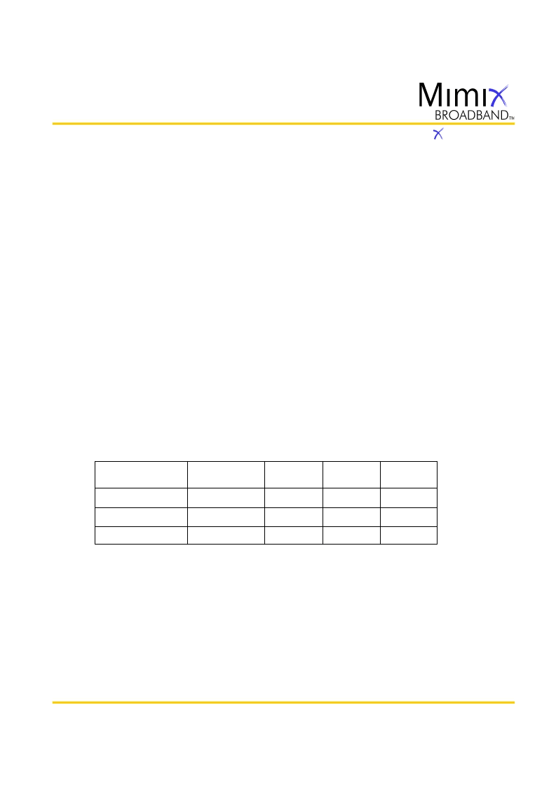
MTTF Tables (TBD)
Backplate
Temperature
55 deg Celsius
75 deg Celsius
95 deg Celsius
Channel
Temperature
deg Celsius
deg Celsius
deg Celsius
FITs
E+
E+
E+
MTTF Hours
E+
E+
E+
Rth
C/
W
C/
W
C/
W
Bias Conditions:
Vd1=Vd2=Vd3=5.0V, Vss=-5.0V, Id1=230mA, Id2=140mA, Id3=75mA, Iss=50mA
These numbers were calculated based on accelerated life test information and thermal model analysis received from the fabricating foundry.
App Note [1] Biasing
- As shown in the bonding diagram, this device is operated by separately biasing Vd(1,2,3)=5.0V,
Vss=-5.0V, Id1=230mA, Id2=140mA, Id3=75mA and Iss=50mA. Additionally, a mixer and doubler bias are also required
with Vg3=Vg4=-0.5V. Adjusting Vg3 and Vg4 above or below this value can adversely affect conversion gain, LO/RF
isolation and intercept point performance. Gain control can be adjusted by varying Vg1 from 0.0 to -1.2 V with 0.0 V
providing minimum attenuation and -1.2 V providing maximum attenuation. It is also recommended to use active
biasing to keep the currents constant as the RF power and temperature vary; this gives the most reproducible results.
Depending on the supply voltage available and the power dissipation constraints, the bias circuit may be a single
transistor or a low power operational amplifier, with a low value resistor in series with the drain supply used to sense the
current. The gate of the pHEMT is controlled to maintain correct drain current and thus drain voltage. The typical gate
voltage needed to do this is -0.2V. Typically the gate is protected with Silicon diodes to limit the applied voltage. Also,
make sure to sequence the applied voltage to ensure negative gate bias is available before applying the positive drain
supply.
App Note [2] Bias Arrangement
-
For Parallel Stage Bias (Recommended for general applications) -- The same as Individual Stage Bias but all the drain or
gate pad DC bypass capacitors ( 100-200 pF) can be combined. Additional DC bypass capacitance ( 0.01 uF) is also
recommended to all DC or combination (if gate or drains are tied together) of DC bias pads.
For Individual Stage Bias -- Each DC pad (Vd1,2,3, Vss, and Vg1,2,3,4) needs to have DC bypass capacitance ( 100-200 pF)
as close to the device as possible. Additional DC bypass capacitance ( 0.01 uF) is also recommended.
Mimix Broadband, Inc., 10795 Rockley Rd., Houston, Texas 77099
Tel: 281.988.4600 Fax: 281.988.4615 mimixbroadband.com
Characteristic Data and Specifications are subject to change without notice.
2007 Mimix Broadband, Inc.
Export of this item may require appropriate export licensing from the U.S. Government. In purchasing these parts, U.S. Domestic customers accept
their obligation to be compliant with U.S. Export Laws.
March 2007 - Rev 01-Mar-07
U1009-BD
相關(guān)PDF資料 |
PDF描述 |
|---|---|
| XU1009-BD-EV1 | 18.0-36.0 GHz GaAs MMIC Transmitter |
| XX1000-BD | 7.5-25.0/15.0-50.0 GHz GaAs MMIC Active Doubler |
| XX1000-BD-000V | 7.5-25.0/15.0-50.0 GHz GaAs MMIC Active Doubler |
| XX1000-BD-EV1 | 7.5-25.0/15.0-50.0 GHz GaAs MMIC Active Doubler |
| XX1000-QT_07 | 7.5-22.5/15.0-45.0 GHz Active Doubler QFN, 3x3 mm |
相關(guān)代理商/技術(shù)參數(shù) |
參數(shù)描述 |
|---|---|
| XU1009-BD-EV1 | 制造商:MIMIX 制造商全稱:MIMIX 功能描述:18.0-36.0 GHz GaAs MMIC Transmitter |
| XU1009-V | 制造商:M/A-COM Technology Solutions 功能描述:RF TRANSMITTER MODULE |
| XU1010-BD | 制造商:MIMIX 制造商全稱:MIMIX 功能描述:16.0-36.0 GHz GaAs MMIC Up-Converter |
| XU1010-BD_09 | 制造商:MIMIX 制造商全稱:MIMIX 功能描述:17.0-34.0 GHz GaAs MMIC |
| XU1010-QH | 制造商:MIMIX 制造商全稱:MIMIX 功能描述:16.0-36.0 GHz Up-Converter QFN, 4x4mm |
發(fā)布緊急采購(gòu),3分鐘左右您將得到回復(fù)。