- 您現(xiàn)在的位置:買賣IC網(wǎng) > PDF目錄376453 > XR-T7295IW (EXAR CORP) DS3/Sonet STS-1 Integrated Line Receiver PDF資料下載
參數(shù)資料
| 型號(hào): | XR-T7295IW |
| 廠商: | EXAR CORP |
| 元件分類: | 數(shù)字傳輸電路 |
| 英文描述: | DS3/Sonet STS-1 Integrated Line Receiver |
| 中文描述: | RECEIVER, PDSO20 |
| 封裝: | 0.300 INCH, PLASTIC, SOJ-20 |
| 文件頁數(shù): | 10/20頁 |
| 文件大?。?/td> | 226K |
| 代理商: | XR-T7295IW |
XR-T7295
10
Rev. 1.05
OUTPUT JITTER
The total jitter appearing on the RCLK output during
normal operation consists of two components. First,
some jitter appears on RCLK because of jitter on the
incoming signal. (The next section discusses the jitter
transfer characteristic, which describes the relationship
between input and output jitter.) Second, noise sources
within the XR-T7295 device and noise sources that are
coupled into the device through the power supplies and
data pattern dependent jitter due to misequalization of the
input signal, all create jitter on RCLK. The magnitude of
this internally generated jitter is a function of the PLL
bandwidth, which in turn is a function of the input 1s
density. For higher 1s density, the amount of generated
jitter decreases. Generated jitter also depends on the
quality of the power supply bypassing networks used.
Figure 12shows the suggested bypassing network, and
Table 6lists the typical generated jitter performance.
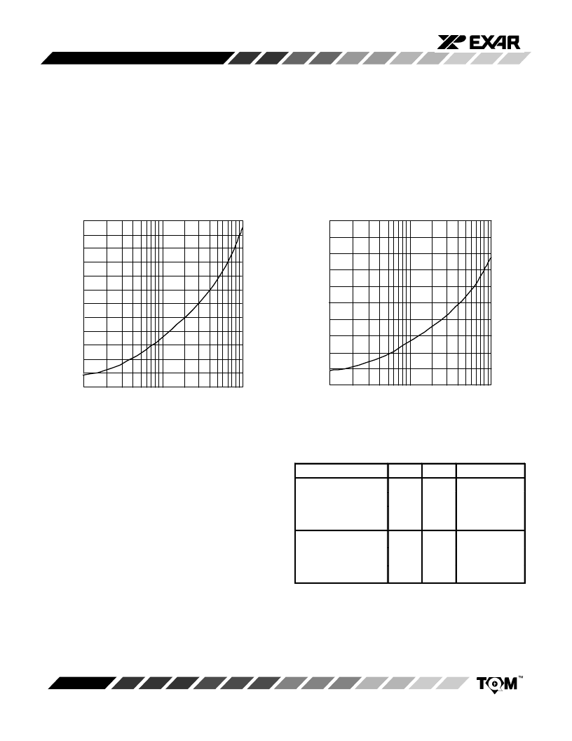
Figure 7. Loss Characteristic of 728A
Coaxial Cable (450 ft.)
Figure 8. Phase Characteristic of 728A
Coaxial Cable (450 ft.)
01.0
2.0
5.0 10
Frequency (MHz)
12
10
20
50
100
0
1.0
2.0
5.0
10
Frequency (MHz)
100
80
60
40
20
20
50
100
L
P
JITTER TRANSFER CHARACTERISTIC
The jitter transfer characteristic indicates the fraction of
input jitter that reaches the RCLK output as a function of
input jitter frequency. Table 6shows Important jitter
transfer characteristic parameters. Figure 9also shows a
typical characteristic, with the operating conditions as
described in Table 6. Although existing standards do not
specify jitter transfer characteristic requirements, the
XR-T7295 information is provided here to assist in
evaluation of the device.
Parameter
Typ
Max
Unit
Generated Jitter
1
All 1s pattern
1.0
ns peak-to-peak
Repetitive “100”
pattern
Jitter Transfer
2
Characteristic
Peaking
f 3dB
1.5
ns peak-to-peak
0.05
0 05
205
0.1
dB
kHz
Notes
1
Repetitive input data pattern at nominal DSX-3 level with
V
DD
= 5V T
A
= 25
°
C.
2
Repetitive “100 ” input at nominal DSX-3 level with V
DD
= 5V,
T
A
= 25
°
C.
Table 6. Generated Jitter and Jitter Transfer
Characteristics
相關(guān)PDF資料 |
PDF描述 |
|---|---|
| XR-T7296 | DS3/STS-1, E3 Integrated Line Transmitter |
| XR-T7296IP | DS3/STS-1, E3 Integrated Line Transmitter |
| XR-T7296IW | DS3/STS-1, E3 Integrated Line Transmitter |
| XR16C2850 | 3.3V AND 5V DUART WITH 128-BYTE FIFO |
| XR16C2850CJ44 | 3.3V AND 5V DUART WITH 128-BYTE FIFO |
相關(guān)代理商/技術(shù)參數(shù) |
參數(shù)描述 |
|---|---|
| XR-T7295SIP | 制造商:未知廠家 制造商全稱:未知廠家 功能描述:ATM/SONET Receiver |
| XR-T7295SIW | 制造商:未知廠家 制造商全稱:未知廠家 功能描述:ATM/SONET Receiver |
| XR-T7295TIP | 制造商:未知廠家 制造商全稱:未知廠家 功能描述:PCM Receiver |
| XR-T7295TIW | 制造商:未知廠家 制造商全稱:未知廠家 功能描述:PCM Receiver |
| XRT7296 | 制造商:EXAR 制造商全稱:EXAR 功能描述:INTEGRATED LINE TRANSMITTER |
發(fā)布緊急采購,3分鐘左右您將得到回復(fù)。