- 您現(xiàn)在的位置:買(mǎi)賣(mài)IC網(wǎng) > PDF目錄225573 > XD010-04S-D4FY (SIRENZA MICRODEVICES INC) 350 MHz - 600 MHz RF/MICROWAVE WIDE BAND HIGH POWER AMPLIFIER PDF資料下載
參數(shù)資料
| 型號(hào): | XD010-04S-D4FY |
| 廠(chǎng)商: | SIRENZA MICRODEVICES INC |
| 元件分類(lèi): | 放大器 |
| 英文描述: | 350 MHz - 600 MHz RF/MICROWAVE WIDE BAND HIGH POWER AMPLIFIER |
| 封裝: | GREEN, D4F, 4 PIN |
| 文件頁(yè)數(shù): | 1/5頁(yè) |
| 文件大小: | 142K |
| 代理商: | XD010-04S-D4FY |
1625-1675The information provided herein is believed to be reliable at press time. Sirenza Microdevices assumes no responsibility for inaccuracies or omissions. Sirenza Microdevices assumes no responsibility for the use of this information, and
all such information shall be entirely at the user’s own risk. Prices and specifications are subject to change without notice. No patent rights or licenses to any of the circuits described herein are implied or granted to any thrid party. Sirenza Microdevices
does not authorize or warrant any Sirenza Microdevices product for use in life-support devices and/or systems. Copyright 2003 Sirenza Microdevices, Inc. All worldwide rights reserved.
303 S. Technology Court,
Phone: (800) SMI-MMIC
http://www.sirenza.com
Broomfield, CO 80021
1
EDS-104259 Rev E
Sirenza Microdevices’ XD010-04S-D4F 12W power module is a robust
broadband 2-stage Class A/AB amplifier, suitable for use as a power ampli-
fier driver or output stage. The power transistors are fabricated using
Sirenza's latest, high performance LDMOS process. It is a drop-in, no-
tune, solution for high power applications requiring high efficiency, excel-
lent linearity, and unit-to-unit repeatability. Internal bias current compensa-
tion ensures stable performance over a wide temperature range. It is
internally matched to 50 ohms.
Key Specifications
Symbol
Parameter
Unit
Min.
Typ.
Max.
Frequency
Frequency of Operation
MHz
350
-
600
P1dB
Output Power at 1dB Compression, 450MHz
W
-
12
-
Gain
Gain at 10W Output Power, 450MHz
dB
30
32
-
Gain Flatness
Peak to Peak Gain Variation, 350 - 600MHz
dB
-
1.0
2.0
IRL
Input Return Loss 1W Output Power, 350 - 600MHz
dB
10
15
-
Efficiency
Drain Efficiency at 10W CW, 350-600MHz
%
26
30
-
Linearity
3rd Order IMD at 10W PEP (Two Tone), 450MHz & 451MHz
dBc
-
-32
-28
Delay
Signal Delay from Pin 1 to Pin 4
nS
-
2.5
-
Phase Linearity
Deviation from Linear Phase (Peak to Peak)
Deg
-
0.5
-
Frequency
Frequency of Operation
MHz
350
-
600
RTH, j-l
Thermal Resistance Stage 1 (Junction-to-Case)
C/W
11
RTH, j-2
Thermal Resistance Stage 2 (Junction-to-Case)
C/W
4
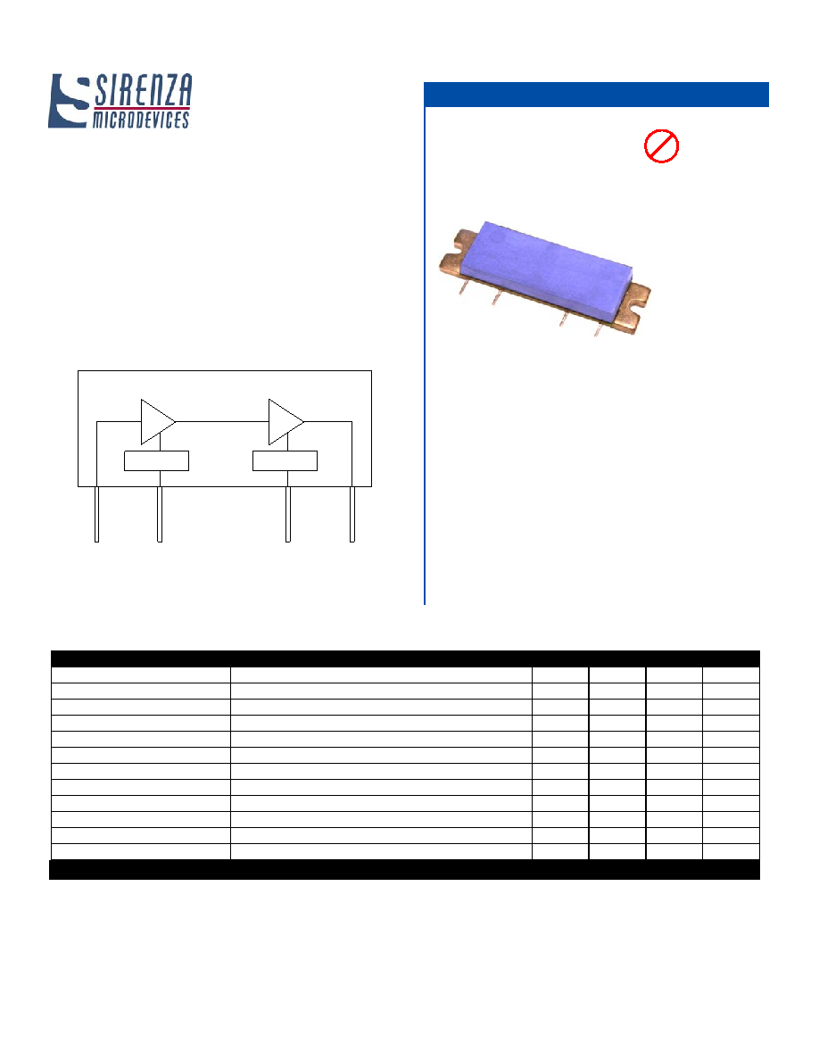
XD010-04S-D4F
350-600 MHz Class AB
12W Power Amplifier Module
Product Features
Applications
Available in RoHS compliant packaging
50 W RF impedance
12W Output P
1dB
Single Supply Operation : Nominally 28V
High Gain: 32 dB at 450 MHz
High Efficiency: 30% at 450 MHz
Robust 8000V ESD (HBM), Class 3B
XeMOS II LDMOS FETS
Temperature Compensation
DTV
Public Service
Wireless Infrastructure
Military Communications
Product Description
Bias
Network
Temperature
Compensation
VD2
D1
V
RF out
RF in
Stage 2
Stage 1
1
23
4
Case Flange = Ground
Test Conditions Zin = Zout = 50, VDD = 28.0V, IDQ1 = 230 mA, IDQ2 =150 mA, TFlange = 25C
Functional Block Diagram
XD010-04S-D4FY Pb
RoHS Compliant
& Green Package
相關(guān)PDF資料 |
PDF描述 |
|---|---|
| XF2B-2145-31A | 21 CONTACT(S), FEMALE, STRAIGHT FFC/FPC CONNECTOR, SOLDER |
| XF2B-2545-31A | 25 CONTACT(S), FEMALE, STRAIGHT FFC/FPC CONNECTOR, SOLDER |
| XF2B-2745-31A | 27 CONTACT(S), FEMALE, STRAIGHT FFC/FPC CONNECTOR, SOLDER |
| XF2B-3145-31A | 31 CONTACT(S), FEMALE, STRAIGHT FFC/FPC CONNECTOR, SOLDER |
| XF2B-3345-31A | 33 CONTACT(S), FEMALE, STRAIGHT FFC/FPC CONNECTOR, SOLDER |
相關(guān)代理商/技術(shù)參數(shù) |
參數(shù)描述 |
|---|---|
| XD010-12S-D4F | 制造商:RF Micro Devices Inc 功能描述:MODULE POWER AMP LDMOS 10W AB |
| XD010-14S-D4F | 制造商:RF Micro Devices Inc 功能描述:MODULE POWER AMP LDMOS 10W A/AB |
| XD010-22S-D2F | 制造商:RF Micro Devices Inc 功能描述:MODULE POWER AMP LDMOS 10W A/AB |
| XD010-24S-D2F | 制造商:RF Micro Devices Inc 功能描述:MODULE POWER AMP LDMOS 10W A/AB |
| XD010-42S-D4F | 制造商:RF Micro Devices Inc 功能描述:MODULE POWER AMP LDMOS 10W A |
發(fā)布緊急采購(gòu),3分鐘左右您將得到回復(fù)。