- 您現(xiàn)在的位置:買賣IC網(wǎng) > PDF目錄375019 > XCV2600E-8FG240I (Xilinx, Inc.) Virtex⑩-E 1.8 V Field Programmable Gate Arrays PDF資料下載
參數(shù)資料
| 型號: | XCV2600E-8FG240I |
| 廠商: | Xilinx, Inc. |
| 英文描述: | Virtex⑩-E 1.8 V Field Programmable Gate Arrays |
| 中文描述: | 的Virtex⑩娥1.8伏現(xiàn)場可編程門陣列 |
| 文件頁數(shù): | 4/5頁 |
| 文件大小: | 87K |
| 代理商: | XCV2600E-8FG240I |
Virtex-E Ordering Information
Revision History
The following table shows the revision history for this document.
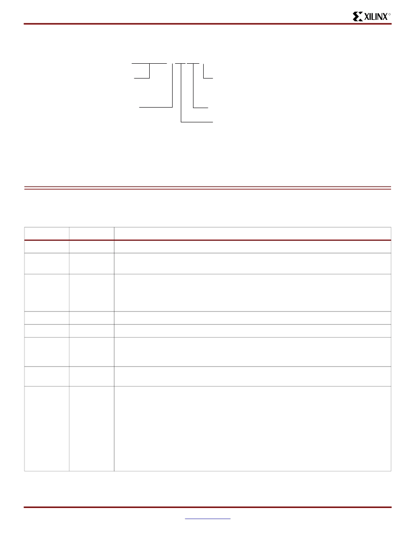
Figure 1:
Ordering Information
Date
Version
Revision
12/7/99
1.0
Initial Xilinx release.
1/10/00
1.1
Re-released with spd.txt v. 1.18, FG860/900/1156 package information, and additional DLL,
Select RAM and SelectI/O information.
1/28/00
1.2
Added Delay Measurement Methodology table, updated SelectI/O section, Figures 30, 54,
& 55, text explaining Table 5, T
BYP
values, buffered Hex Line info, p. 8, I/O Timing
Measurement notes, notes for Tables 15, 16, and corrected F1156 pinout table footnote
references.
2/29/00
1.3
Updated pinout tables, V
CC
page 20, and corrected Figure 20.
5/23/00
1.4
Correction to table on p. 22.
7/10/00
1.5
Numerous minor edits.
Data sheet upgraded to Preliminary.
Preview -8 numbers added to
Virtex-E Electrical Characteristics
tables.
Reformatted entire document to follow new style guidelines.
Changed speed grade
values in tables on pages 35-37.
Min values added to
Virtex-E Electrical Characteristics
tables.
XCV2600E and XCV3200E numbers added to
Virtex-E Electrical Characteristics
tables (Module 3).
Corrected user I/O count for XCV100E device in Table 1 (Module 1).
Changed several pins to
“
No Connect in the XCV100E
“
and removed duplicate V
CCINT
pins in Table ~ (Module 4).
Changed pin J10 to
“
No connect in XCV600E
”
in Table 74 (Module 4).
Changed pin J30 to
“
VREF option only in the XCV600E
”
in Table 74 (Module 4).
Corrected pair 18 in Table 75 (Module 4) to be
“
AO in the XCV1000E, XCV1600E
“
.
8/1/00
1.6
9/20/00
1.7
Example: XCV300E-6PQ240C
Device Type
Temperature Range
C = Commercial (Tj = 0 C to +85 C)
I = Industrial (Tj = -40 C to +100 C)
Number of Pins
Package Type
BG = Ball Grid Array
FG = Fine Pitch Ball Grid Array
HQ = High Heat Dissipation
Speed Grade
(-6, -7, -8)
DS022_043_072000
相關(guān)PDF資料 |
PDF描述 |
|---|---|
| XCV2600E-8HQ240C | Virtex⑩-E 1.8 V Field Programmable Gate Arrays |
| XCV2600E-8HQ240I | Virtex⑩-E 1.8 V Field Programmable Gate Arrays |
| XCV300E-6BG240C | GT 7C 7#16S SKT PLUG |
| XCV600E-6FG240C | ER 4C 4#8 PIN PLUG |
| XCV600E-6FG240I | GT 4C 4#8 PIN PLUG |
相關(guān)代理商/技術(shù)參數(shù) |
參數(shù)描述 |
|---|---|
| XCV2600E-8HQ240C | 制造商:XILINX 制造商全稱:XILINX 功能描述:Virtex⑩-E 1.8 V Field Programmable Gate Arrays |
| XCV2600E-8HQ240I | 制造商:XILINX 制造商全稱:XILINX 功能描述:Virtex⑩-E 1.8 V Field Programmable Gate Arrays |
| XCV300 | 制造商:XILINX 制造商全稱:XILINX 功能描述:Field Programmable Gate Arrays |
| XCV300-4BG256C | 制造商:XILINX 制造商全稱:XILINX 功能描述:Field Programmable Gate Arrays |
| XCV300-4BG256I | 制造商:XILINX 制造商全稱:XILINX 功能描述:Field Programmable Gate Arrays |
發(fā)布緊急采購,3分鐘左右您將得到回復(fù)。