- 您現(xiàn)在的位置:買賣IC網(wǎng) > PDF目錄372876 > XC9511D1463 (TOREX SEMICONDUCTOR LTD.) Synchronous Step-Down DC/DC Converter with built-in LDO Regulator in parallel plus Voltage Detector PDF資料下載
參數(shù)資料
| 型號: | XC9511D1463 |
| 廠商: | TOREX SEMICONDUCTOR LTD. |
| 英文描述: | Synchronous Step-Down DC/DC Converter with built-in LDO Regulator in parallel plus Voltage Detector |
| 中文描述: | 同步降壓型DC / DC轉(zhuǎn)換器內(nèi)置LDO的同時加電壓檢測器調(diào)節(jié)器 |
| 文件頁數(shù): | 8/35頁 |
| 文件大小: | 3471K |
| 代理商: | XC9511D1463 |
第1頁第2頁第3頁第4頁第5頁第6頁第7頁當(dāng)前第8頁第9頁第10頁第11頁第12頁第13頁第14頁第15頁第16頁第17頁第18頁第19頁第20頁第21頁第22頁第23頁第24頁第25頁第26頁第27頁第28頁第29頁第30頁第31頁第32頁第33頁第34頁第35頁
8/35
XC9511
Series
FOSC
L
1.2MHz
4.7
μ
H
(CDRH4D28C, SUMIDA)
10
μ
H
(CDRH5D28, SUMIDA)
22
μ
H
(CDRH6D28, SUMIDA)
600KHz
300kHz
C
IN
4.7
μ
F
C
L1
10
μ
F
C
L2
*
2
I
ROUT
<
300mA
I
ROUT
≧
300mA
4.7
μ
F (ceramic, TAIYO YUDEN)
10
μ
F (ceramic, TAIYO YUDEN)
(ceramic, TAIYO YUDEN)
(ceramic, TAIYO YUDEN)
■
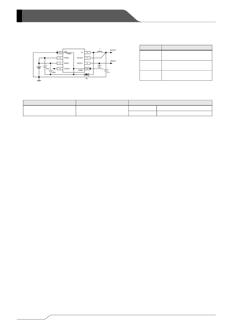
TYPICAL APPLICATION CIRCUIT
SOP-8 (TOP VIEW)
■
OPERATIONAL EXPLANATION
The XC9511 series consists of a synchronous step-down DC/DC converter, a high speed LDO voltage regulator, and a
voltage detector.
●
DC/DC Converter
The series consists of a reference voltage source, ramp wave circuit, error amplifier, PWM comparator, phase
compensation circuit, output voltage adjustment resistors, driver transistor, synchronous switch, current limiter circuit,
U.V.L.O. circuit and others. The series ICs compare, using the error amplifier, the voltage of the internal voltage
reference source with the feedback voltage from the V
OUT
pin through split resistors. Phase compensation is
performed on the resulting error amplifier output, to input a signal to the PWM comparator to determine the turn-on time
during PWM operation. The PWM comparator compares, in terms of voltage level, the signal from the error amplifier
with the ramp wave from the ramp wave circuit, and delivers the resulting output to the buffer driver circuit to cause the
Lx pin to output a switching duty cycle. This process is continuously performed to ensure stable output voltage. The
current feedback circuit monitors the P-channel MOS driver transistor current for each switching operation, and
modulates the error amplifier output signal to provide multiple feedback signals. This enables a stable feedback loop
even when a low ESR capacitor, such as a ceramic capacitor, is used, ensuring stable output voltage.
<Reference Voltage Source>
The reference voltage source provides the reference voltage to ensure stable output voltage of the DC/DC converter.
<Ramp Wave Circuit>
The ramp wave circuit determines switching frequency. The frequency is fixed internally and can be selected from
300kHz, 600 kHz and 1.2 MHz. Clock pulses generated in this circuit are used to produce ramp waveforms needed for
PWM operation, and to synchronize all the internal circuits.
<PWM/PFM>
The XC9511A to C series are PWM control, while the XC9511D to F series can be automatically switched to PWM/PFM
control. The PWM mode of the XC9511A to C series are controlled on a specified frequency from light loads through to
heavy loads. Since the frequency is specified, the composition of a noise filter etc. becomes easy. However, the
efficiency at the time of the light load may become low. The XC9511D to F series can switch to PWM/PFM automatic
switching control. With the automatic PWM/PFM switching control function, the series ICs are automatically switched
from PWM control to PFM control mode under light load conditions. The series cannot control only PFM mode. If
during light load conditions the coil current becomes discontinuous and on-time rate falls lower than 30%, the PFM
circuit operates to output a pulse with 30% of a fixed on-time rate from the Lx pin. During PFM operation with this fixed
on-time rate, pulses are generated at different frequencies according to conditions of the moment. This causes a
reduction in the number of switching operations per unit of time, resulting in efficiency improvement under light load
conditions. However, since pulse output frequency is not constant, consideration should be given if a noise filter or the
like is needed. Necessary conditions for switching to PFM operation depend on input voltage, load current, coil value
and other factors.
SD *1: XB0ASB03A1BR (TOREX)
*1 The DC/DC converter of the XC9511 series automatically switches between synchronous / non-synchronous. The Schottky
diode is not normally needed. However, in cases where high efficiency is required when using the DC/DC converter during light
load while in non-synchronous operation, please connect a Schottky diode externally.
*2 Please pay much attention when external components are selected as recommended value of C
L
2 will be changed by the load
current.
相關(guān)PDF資料 |
PDF描述 |
|---|---|
| XC9511D1464 | Synchronous Step-Down DC/DC Converter with built-in LDO Regulator in parallel plus Voltage Detector |
| XC9511D14C3 | Synchronous Step-Down DC/DC Converter with built-in LDO Regulator in parallel plus Voltage Detector |
| XC9511D14C4 | Synchronous Step-Down DC/DC Converter with built-in LDO Regulator in parallel plus Voltage Detector |
| XC9511E1433 | Synchronous Step-Down DC/DC Converter with built-in LDO Regulator in parallel plus Voltage Detector |
| XC9511E1434 | Synchronous Step-Down DC/DC Converter with built-in LDO Regulator in parallel plus Voltage Detector |
相關(guān)代理商/技術(shù)參數(shù) |
參數(shù)描述 |
|---|---|
| XC9511D1464 | 制造商:TOREX 制造商全稱:Torex Semiconductor 功能描述:Synchronous Step-Down DC/DC Converter with built-in LDO Regulator in parallel plus Voltage Detector |
| XC9511D146SRL | 制造商:TOREX 制造商全稱:Torex Semiconductor 功能描述:Synchronous Step-Down DC/DC Converter with built-in LDO Regulator in parallel plus Voltage Detector |
| XC9511D14C3 | 制造商:TOREX 制造商全稱:Torex Semiconductor 功能描述:Synchronous Step-Down DC/DC Converter with built-in LDO Regulator in parallel plus Voltage Detector |
| XC9511D14C4 | 制造商:TOREX 制造商全稱:Torex Semiconductor 功能描述:Synchronous Step-Down DC/DC Converter with built-in LDO Regulator in parallel plus Voltage Detector |
| XC9511D14CSRL | 制造商:TOREX 制造商全稱:Torex Semiconductor 功能描述:Synchronous Step-Down DC/DC Converter with built-in LDO Regulator in parallel plus Voltage Detector |
發(fā)布緊急采購,3分鐘左右您將得到回復(fù)。