- 您現(xiàn)在的位置:買賣IC網(wǎng) > PDF目錄225573 > XC7K420T-1LFFG1156C (XILINX INC) FPGA, PBGA1156 PDF資料下載
參數(shù)資料
| 型號: | XC7K420T-1LFFG1156C |
| 廠商: | XILINX INC |
| 元件分類: | FPGA |
| 英文描述: | FPGA, PBGA1156 |
| 封裝: | LEAD FREE, FBGA-1156 |
| 文件頁數(shù): | 26/50頁 |
| 文件大小: | 1218K |
| 代理商: | XC7K420T-1LFFG1156C |
第1頁第2頁第3頁第4頁第5頁第6頁第7頁第8頁第9頁第10頁第11頁第12頁第13頁第14頁第15頁第16頁第17頁第18頁第19頁第20頁第21頁第22頁第23頁第24頁第25頁當前第26頁第27頁第28頁第29頁第30頁第31頁第32頁第33頁第34頁第35頁第36頁第37頁第38頁第39頁第40頁第41頁第42頁第43頁第44頁第45頁第46頁第47頁第48頁第49頁第50頁
Kintex-7 FPGAs Data Sheet: DC and Switching Characteristics
DS182 (v1.1) April 1, 2011
Advance Product Specification
32
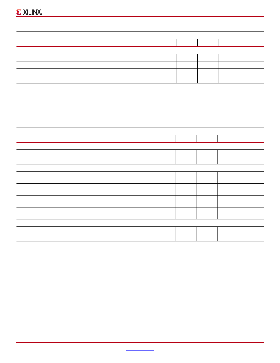
CLB Distributed RAM Switching Characteristics (SLICEM Only)
Set/Reset
TSRMIN
SR input minimum pulse width
0.50
0.75
1.00
ns, Min
TRQ
Delay from SR input to AQ – DQ flip-flops
0.55
0.61
0.71
ns, Max
TCEO
Delay from CE input to AQ – DQ flip-flops
0.44
0.51
0.61
ns, Max
FTOG
Toggle frequency (for export control)
1412
1286
1098
MHz
Notes:
1.
A Zero “0” Hold Time listing indicates no hold ti
me or a negative hold time. Negative values can not be guaranteed “best-case”, but if a “0” is
listed, there is no positive hold time.
2.
These items are of interest for Carry Chain applications.
Table 36: CLB Distributed RAM Switching Characteristics
Symbol
Description
Speed Grade
Units
-3
-2
-1
-1L
Sequential Delays
TSHCKO
Clock to A – B outputs
0.99
1.18
1.46
ns, Max
TSHCKO_1
Clock to AMUX – BMUX outputs
1.26
1.48
1.80
ns, Max
Setup and Hold Times Before/After Clock CLK
TDS_LRAM/TDH_LRAM
A – D inputs to CLK
0.64/
0.21
0.75/
0.23
0.91/
0.26
ns, Min
TAS_LRAM/TAH_LRAM
Address An inputs to clock
0.17/
0.46
0.21/
0.50
0.26/
0.58
ns, Min
TWS_LRAM/TWH_LRAM WE input to clock
0.27/
0.03
0.33/
0.03
0.41/
0.03
ns, Min
TCECK_LRAM/
TCKCE_LRAM
CE input to CLK
0.28/
0.02
0.34/
0.02
0.42/
0.02
ns, Min
Clock CLK
TMPW_LRAM
Minimum pulse width
0.77
0.90
1.09
ns, Min
TMCP
Minimum clock period
1.53
1.79
2.18
ns, Min
Notes:
1.
A Zero “0” Hold Time listing indicates no hold time or a negative hold time. Negative values cannot be guaranteed “best-case”, but if a “0” is
listed, there is no positive hold time.
2.
TSHCKO also represents the CLK to XMUX output. Refer to TRACE report for the CLK to XMUX path.
Table 35: CLB Switching Characteristics (Cont’d)
Symbol
Description
Speed Grade
Units
-3
-2
-1
-1L
相關PDF資料 |
PDF描述 |
|---|---|
| XC7K420T-1LFFG1156E | FPGA, PBGA1156 |
| XC7K420T-1LFFG1156I | FPGA, PBGA1156 |
| XC7K420T-1LFFG901C | FPGA, PBGA900 |
| XC7K420T-1LFFG901E | FPGA, PBGA900 |
| XC7K420T-1LFFG901I | FPGA, PBGA900 |
相關代理商/技術參數(shù) |
參數(shù)描述 |
|---|---|
| XC7K420T-2FF1156C | 制造商:Xilinx 功能描述:KINTEX-7 - Trays 制造商:Xilinx 功能描述:IC FPGA 400 I/O 1156FCBGA |
| XC7K420T-2FF1156I | 制造商:Xilinx 功能描述:KINTEX-7 - Trays 制造商:Xilinx 功能描述:IC FPGA 400 I/O 1156FCBGA |
| XC7K420T-2FF901C | 制造商:Xilinx 功能描述:KINTEX-7 - Trays 制造商:Xilinx 功能描述:IC FPGA 420K KINTEX-7 901FBGA |
| XC7K420T-2FF901I | 制造商:Xilinx 功能描述:KINTEX-7 - Trays 制造商:Xilinx 功能描述:IC FPGA 380 I/O 901FCBGA |
| XC7K420T-2FFG1156C | 制造商:Xilinx 功能描述:IC FPGA 420K KINTEX-7 1156FBGA |
發(fā)布緊急采購,3分鐘左右您將得到回復。