- 您現(xiàn)在的位置:買賣IC網(wǎng) > PDF目錄371340 > XC5215-3BG225I Field Programmable Gate Array (FPGA) PDF資料下載
參數(shù)資料
| 型號: | XC5215-3BG225I |
| 英文描述: | Field Programmable Gate Array (FPGA) |
| 中文描述: | 現(xiàn)場可編程門陣列(FPGA) |
| 文件頁數(shù): | 50/73頁 |
| 文件大?。?/td> | 598K |
| 代理商: | XC5215-3BG225I |
第1頁第2頁第3頁第4頁第5頁第6頁第7頁第8頁第9頁第10頁第11頁第12頁第13頁第14頁第15頁第16頁第17頁第18頁第19頁第20頁第21頁第22頁第23頁第24頁第25頁第26頁第27頁第28頁第29頁第30頁第31頁第32頁第33頁第34頁第35頁第36頁第37頁第38頁第39頁第40頁第41頁第42頁第43頁第44頁第45頁第46頁第47頁第48頁第49頁當(dāng)前第50頁第51頁第52頁第53頁第54頁第55頁第56頁第57頁第58頁第59頁第60頁第61頁第62頁第63頁第64頁第65頁第66頁第67頁第68頁第69頁第70頁第71頁第72頁第73頁
R
XC5200 Series Field Programmable Gate Arrays
7-132
November 5, 1998 (Version 5.2)
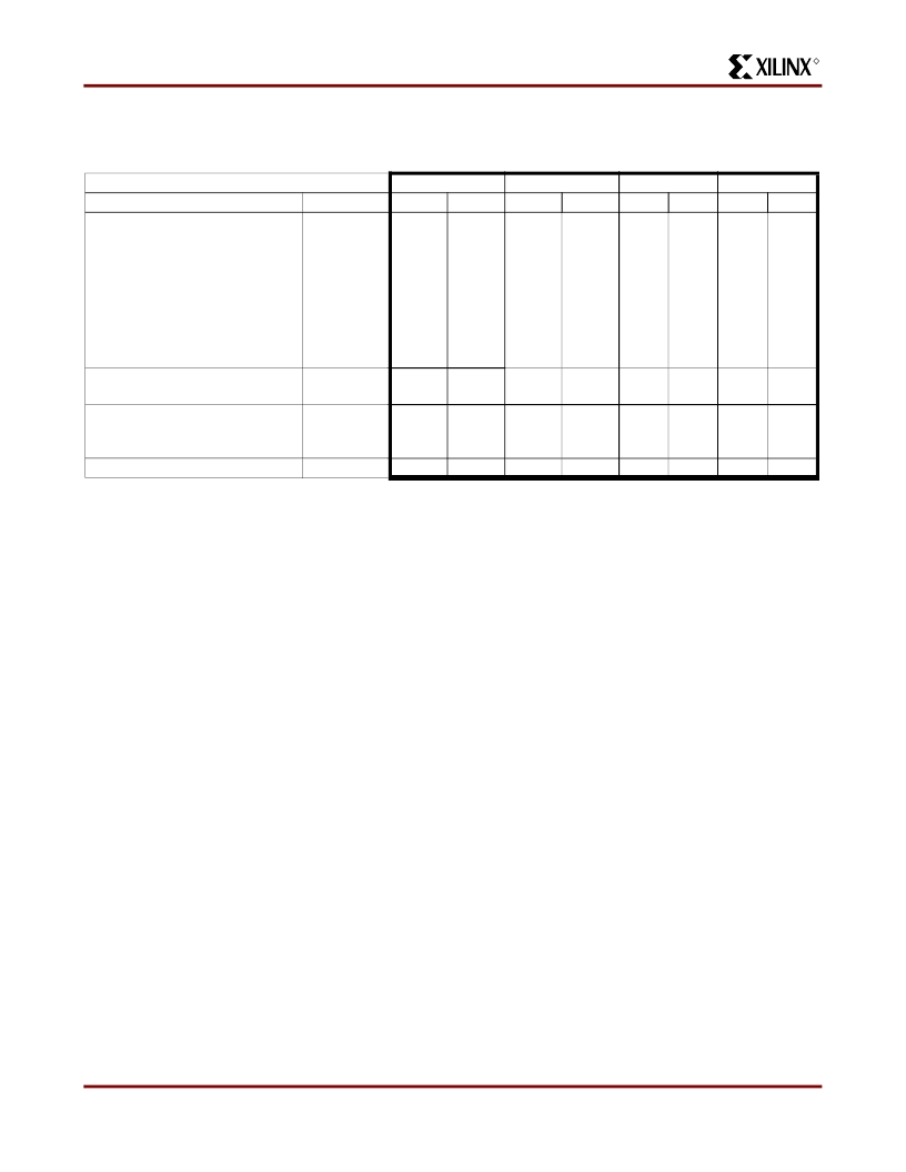
XC5200 Boundary Scan (JTAG) Switching Characteristic Guidelines
The following guidelines reflect worst-case values over the recommended operating conditions. They are expressed in units
of nanoseconds and apply to all XC5200 devices unless otherwise noted.
Speed Grade
Description
Setup and Hold
Input (TDI) to clock (TCK)
setup time
Input (TDI) to clock (TCK)
hold time
Input (TMS) to clock (TCK)
setup time
Input (TMS) to clock (TCK)
hold time
Propagation Delay
Clock (TCK) to Pad (TDO)
Clock
Clock (TCK) High
Clock (TCK) Low
F
MAX
(MHz)
-6
-5
-4
-3
Symbol
Min
Max
Min
Max
Min
Max
Min
Max
T
TDITCK
T
TCKTDI
T
TMSTCK
T
TCKTMS
30.0
0
15.0
0
30.0
0
15.0
0
30.0
0
15.0
0
30.0
0
15.0
0
T
TCKPO
30.0
30.0
30.0
30.0
T
TCKH
T
TCKL
F
MAX
30.0
30.0
30.0
30.0
30.0
30.0
30.0
30.0
10.0
10.0
10.0
10.0
Note 1:
Input pad setup and hold times are specified with respect to the internal clock.
發(fā)布緊急采購,3分鐘左右您將得到回復(fù)。