- 您現(xiàn)在的位置:買賣IC網(wǎng) > PDF目錄374983 > XC3042A-7TQ144C (XILINX INC) Field Programmable Gate Arrays (XC3000A/L, XC3100A/L) PDF資料下載
參數(shù)資料
| 型號: | XC3042A-7TQ144C |
| 廠商: | XILINX INC |
| 元件分類: | FPGA |
| 英文描述: | Field Programmable Gate Arrays (XC3000A/L, XC3100A/L) |
| 中文描述: | FPGA, 144 CLBS, 2000 GATES, 113 MHz, PQFP144 |
| 封裝: | PLASTIC, TQFP-144 |
| 文件頁數(shù): | 9/50頁 |
| 文件大?。?/td> | 474K |
| 代理商: | XC3042A-7TQ144C |
第1頁第2頁第3頁第4頁第5頁第6頁第7頁第8頁當(dāng)前第9頁第10頁第11頁第12頁第13頁第14頁第15頁第16頁第17頁第18頁第19頁第20頁第21頁第22頁第23頁第24頁第25頁第26頁第27頁第28頁第29頁第30頁第31頁第32頁第33頁第34頁第35頁第36頁第37頁第38頁第39頁第40頁第41頁第42頁第43頁第44頁第45頁第46頁第47頁第48頁第49頁第50頁
2-111
switch connections to block inputs are unidirec-
tional, as are block outputs, they are usable only for
block input connection and not for routing.
Figure 8
illustrates routing access to logic block input variables,
control inputs and block outputs. Three types of metal
resources are provided to accommodate various network
interconnect requirements.
General Purpose Interconnect
Direct Connection
Longlines (multiplexed busses and wide AND gates)
General Purpose Interconnect
General purpose interconnect, as shown in Figure 9,
consists of a grid of five horizontal and five vertical metal
segments located between the rows and columns of logic
and IOBs. Each segment is the height or width of a logic
block. Switching matrices join the ends of these segments
and allow programmed interconnections between the
metal grid segments of adjoining rows and columns. The
switches of an unprogrammed device are all non-
conducting. The connections through the switch matrix
may be established by the automatic routing or by using
Editnet to select the desired pairs of matrix pins to be
connected or disconnected. The legitimate switching
matrix combinations for each pin are indicated in Figure 10
and may be highlighted by the use of the Show-Matrix
command in the XACT system.
asynchronous RD which, when enabled and High, is
dominant over clocked inputs. All flip-flops are reset by the
active-Low chip input, RESET, or during the configuration
process. The flip-flops share the enable clock (EC) which,
when Low, recirculates the flip-flops’ present states and
inhibits response to the data-in or combinatorial function
inputs on a CLB. The user may enable these control inputs
and select their sources. The user may also select the
clock net input (K), as well as its active sense within each
CLB. This programmable inversion eliminates the need to
route both phases of a clock signal throughout the device.
Flexible routing allows use of common or individual CLB
clocking.
The combinatorial-logic portion of the CLB uses a 32 by 1
look-up table to implement Boolean functions. Variables
selected from the five logic inputs and two internal block
flip-flops are used as table address inputs. The combina-
torial propagation delay through the network is indepen-
dent of the logic function generated and is spike free for
single input variable changes. This technique can gener-
ate two independent logic functions of up to four variables
each as shown in Figure 5a, or a single function of five
variables as shown in Figure 5b, or some functions of
seven variables as shown in Figure 5c. Figure 6 shows a
modulo-8 binary counter with parallel enable. It uses one
CLB of each type. The partial functions of six or seven
variables are implemented using the input variable (E) to
dynamically select between two functions of four different
variables. For the two functions of four variables each, the
independent results (F and G) may be used as data inputs
to either flip-flop or either logic block output. For the single
function of five variables and merged functions of six or
seven variables, the F and G outputs are identical. Sym-
metry of the F and G functions and the flip-flops allows the
interchange of CLB outputs to optimize routing efficiencies
of the networks interconnecting the CLBs and IOBs.
Programmable Interconnect
Programmable-interconnection resources in the Logic
Cell Array provide routing paths to connect inputs and
outputs of the IOBs and CLBs into logic networks. Inter-
connections between blocks are composed of a two-layer
grid of metal segments. Specially designed pass transis-
tors, each controlled by a configuration bit, form program-
mable interconnect points (PIPs) and switching matrices
used to implement the necessary connections between
selected metal segments and block pins. Figure 7 is an
example of a routed net. The XACT development system
provides automatic routing of these interconnections. In-
teractive routing (Editnet) is also available for design
optimization. The inputs of the CLBs or IOBs are multiplex-
ers which can be programmed to select an input network
from the adjacent interconnect segments.
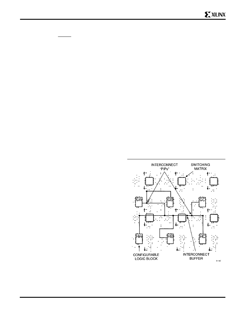
Since the
Figure 7.
An XACT view of routing resources used to form a typical
interconnection network from CLB GA.
相關(guān)PDF資料 |
PDF描述 |
|---|---|
| XC3042A-7TQ144I | Field Programmable Gate Arrays (XC3000A/L, XC3100A/L) |
| XC3164A-3PC84I | Field Programmable Gate Arrays (XC3000A/L, XC3100A/L) |
| XC3164A-3PQ160C | Field Programmable Gate Arrays (XC3000A/L, XC3100A/L) |
| XC3164A-3PQ160I | Field Programmable Gate Arrays (XC3000A/L, XC3100A/L) |
| XC3164A-3TQ144C | Field Programmable Gate Arrays (XC3000A/L, XC3100A/L) |
相關(guān)代理商/技術(shù)參數(shù) |
參數(shù)描述 |
|---|---|
| XC3042A-7TQ144I | 制造商:XILINX 制造商全稱:XILINX 功能描述:Field Programmable Gate Arrays (XC3000A/L, XC3100A/L) |
| XC3042A-7VQ100C | 功能描述:IC FIELD PROG GATE ARRAY 100 PIN RoHS:否 類別:集成電路 (IC) >> 嵌入式 - FPGA(現(xiàn)場可編程門陣列) 系列:XC3000A/L 產(chǎn)品變化通告:XC4000(E,L) Discontinuation 01/April/2002 標(biāo)準(zhǔn)包裝:24 系列:XC4000E/X LAB/CLB數(shù):100 邏輯元件/單元數(shù):238 RAM 位總計(jì):3200 輸入/輸出數(shù):80 門數(shù):3000 電源電壓:4.5 V ~ 5.5 V 安裝類型:表面貼裝 工作溫度:-40°C ~ 100°C 封裝/外殼:120-BCBGA 供應(yīng)商設(shè)備封裝:120-CPGA(34.55x34.55) |
| XC3042A-7VQ100I | 制造商:Xilinx 功能描述: |
| XC3042B | 制造商:未知廠家 制造商全稱:未知廠家 功能描述: |
| XC3042L | 制造商:XILINX 制造商全稱:XILINX 功能描述:Field Programmable Gate Arrays |
發(fā)布緊急采購,3分鐘左右您將得到回復(fù)。