- 您現(xiàn)在的位置:買(mǎi)賣(mài)IC網(wǎng) > PDF目錄371302 > X9430WV24I-2.7 Dual Digitally Controlled Potentiometer (XDCP⑩) with Operational Amplifier PDF資料下載
參數(shù)資料
| 型號(hào): | X9430WV24I-2.7 |
| 元件分類(lèi): | 數(shù)字電位計(jì) |
| 英文描述: | Dual Digitally Controlled Potentiometer (XDCP⑩) with Operational Amplifier |
| 中文描述: | 雙數(shù)字電位器(數(shù)字電位器⑩)的運(yùn)算放大器 |
| 文件頁(yè)數(shù): | 4/21頁(yè) |
| 文件大小: | 881K |
| 代理商: | X9430WV24I-2.7 |
第1頁(yè)第2頁(yè)第3頁(yè)當(dāng)前第4頁(yè)第5頁(yè)第6頁(yè)第7頁(yè)第8頁(yè)第9頁(yè)第10頁(yè)第11頁(yè)第12頁(yè)第13頁(yè)第14頁(yè)第15頁(yè)第16頁(yè)第17頁(yè)第18頁(yè)第19頁(yè)第20頁(yè)第21頁(yè)

X9430
– Preliminary Information
Characteristics subject to change without notice.
4 of 21
REV 1.0 6/20/00
www.xicor.com
Potentiometer/Array Description
The X9430 is comprised of two resistor arrays and two
operational amplifiers. Each array contains 63 discrete
resistive segments that are connected in series. The
physical ends of each array are equivalent to the fixed
terminals of a mechanical potentiometer (R
H
and R
L
).
At both ends of each array and between each resistor
segment is a CMOS switch connected to the wiper
(R
W
) output. Within each individual array only one
switch may be turned on at a time. These switches are
controlled by a volatile wiper counter register (WCR).
The six bits of the WCR are decoded to select, and
enable, one of sixty-four switches.
The WCR may be written directly, or it can be changed
by transferring the contents of one of four associated
data registers into the WCR. These data registers and
the WCR can be read and written by the host system.
Operational Amplifier
The voltage operational amplifiers are CMOS rail-to-rail
output general purpose amplifiers. They are designed
to operate from dual (±) power supplies. The amplifiers
may be configured like any standard amplifier. All pins
are externally available to allow connection with the
potentiometers or as stand alone amplifiers.
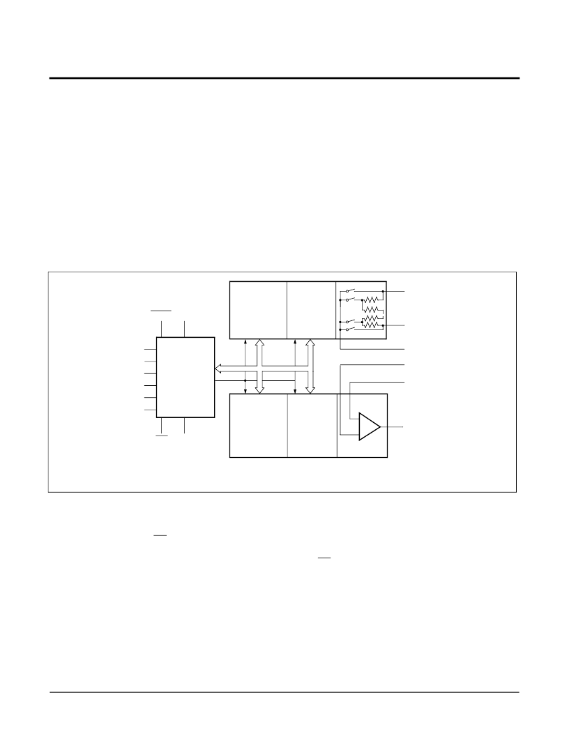
Detailed Block Diagram
(One of 2 Circuits)
V
OUT (0,1)
(DR0-DR3)
0,1
Control and
Memory
CS
SCK
SO
SI
A1
A0
V
H (0,1)
V
L (0,1)
WP
V
W (0,1)
V
N (0,1)
+
–
WCR
0,1
(DR0-DR3)
0,1
V
INV (0,1)
V
SS
V
CC
HOLD
WCR0
WCR1
Write in Process
The contents of the data registers are saved to nonvol-
atile memory when the CS pin goes from LOW to
HIGH after a complete write sequence is received by
the device. The progress of this internal write opera-
tion can be monitored by a write in process bit (WIP).
The WIP bit is read with a read status command.
INSTRUCTIONS AND PROGRAMMING
Identification (ID) Byte
The first byte sent to the X9430 from the host, follow-
ing a CS going HIGH to LOW, is called the identifica-
tion byte. The most significant four bits of the slave
address are a device type identifier, for the X9430 this
is fixed as 0101[B] (refer to Figure 1).
相關(guān)PDF資料 |
PDF描述 |
|---|---|
| X9430WV24M2.7 | Interface IC |
| X9430WS24M | Interface IC |
| X9430WS24M2.7 | Interface IC |
| X9430WV24M | Interface IC |
| X9430WV24 | Dual Digitally Controlled Potentiometer (XDCP) with Operational Amplifier |
相關(guān)代理商/技術(shù)參數(shù) |
參數(shù)描述 |
|---|---|
| X9430WV24M | 制造商:未知廠家 制造商全稱(chēng):未知廠家 功能描述:Interface IC |
| X9430WV24M2.7 | 制造商:未知廠家 制造商全稱(chēng):未知廠家 功能描述:Interface IC |
| X9438 | 制造商:INTERSIL 制造商全稱(chēng):Intersil Corporation 功能描述:Dual Digitally Controlled Potentiometer (XDCP) with Operational Amplifier |
| X9438WP24 | 制造商:INTERSIL 制造商全稱(chēng):Intersil Corporation 功能描述:Dual Digitally Controlled Potentiometer (XDCP) with Operational Amplifier |
| X9438WP24-2.7 | 制造商:INTERSIL 制造商全稱(chēng):Intersil Corporation 功能描述:Dual Digitally Controlled Potentiometer (XDCP) with Operational Amplifier |
發(fā)布緊急采購(gòu),3分鐘左右您將得到回復(fù)。