- 您現(xiàn)在的位置:買賣IC網(wǎng) > PDF目錄371216 > X25642SM-2.7 Advanced SPI Serial E 2 PROM with Block Lock TM Protection PDF資料下載
參數(shù)資料
| 型號: | X25642SM-2.7 |
| 英文描述: | Advanced SPI Serial E 2 PROM with Block Lock TM Protection |
| 中文描述: | 先進的SPI串行E與商標(biāo)保護鎖座2胎膜早破 |
| 文件頁數(shù): | 5/16頁 |
| 文件大?。?/td> | 76K |
| 代理商: | X25642SM-2.7 |

X25642
5
Operational Notes
The X25642 powers-up in the following state:
The device is in the low power standby state.
A HIGH to LOW transition on CS is required to enter
an active state and receive an instruction.
SO pin is high impedance.
The “write enable” latch is reset.
Data Protection
The following circuitry has been included to prevent in-
advertent writes:
The “write enable” latch is reset upon power-up.
A WREN instruction must be issued to set the “write
enable” latch.
CS must come HIGH at the proper clock count in or-
der to start a write cycle.
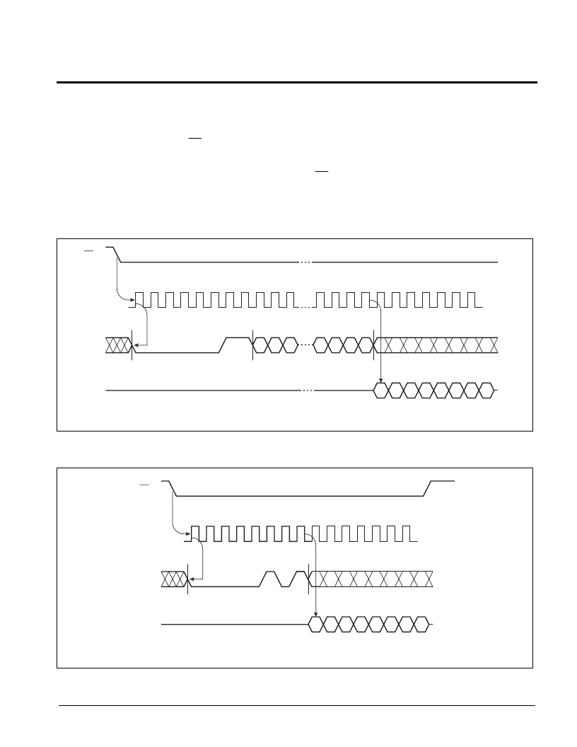
Figure 1. Read E
2
PROM Array Operation Sequence
0
1
2
3
4
5
6
7
8
9
10
20 21 22 23 24 25 26 27 28 29 30
7
6
5
4
3
2
1
0
DATA OUT
CS
SCK
SI
SO
MSB
HIGH IMPEDANCE
INSTRUCTION
16 BIT ADDRESS
15 14 13
3
2
1
0
3132 ILL F03.1
Figure 2. Read Status Register Operation Sequence
0
1
2
3
4
5
6
7
8
9
10
11
12 13 14
7
6
5
4
3
2
1
0
DATA OUT
CS
SCK
SI
SO
MSB
HIGH IMPEDANCE
INSTRUCTION
3132 ILL F04
發(fā)布緊急采購,3分鐘左右您將得到回復(fù)。