- 您現(xiàn)在的位置:買賣IC網(wǎng) > PDF目錄371200 > X24320P 400KHz 2-Wire Serial E2PROM with Block Lock PDF資料下載
參數(shù)資料
| 型號(hào): | X24320P |
| 英文描述: | 400KHz 2-Wire Serial E2PROM with Block Lock |
| 中文描述: | 400kHz的2線串行E2PROM的塊鎖 |
| 文件頁(yè)數(shù): | 1/17頁(yè) |
| 文件大?。?/td> | 85K |
| 代理商: | X24320P |
當(dāng)前第1頁(yè)第2頁(yè)第3頁(yè)第4頁(yè)第5頁(yè)第6頁(yè)第7頁(yè)第8頁(yè)第9頁(yè)第10頁(yè)第11頁(yè)第12頁(yè)第13頁(yè)第14頁(yè)第15頁(yè)第16頁(yè)第17頁(yè)

400KHz 2-Wire Serial E
2
PROM with Block Lock
TM
32K
4K x 8 Bit
7035-1.2 4/25/97 T0/C2/D0 SH
Xicor, 1995, 1996 Patents Pending
Characteristics subject to change without notice
1
X24320
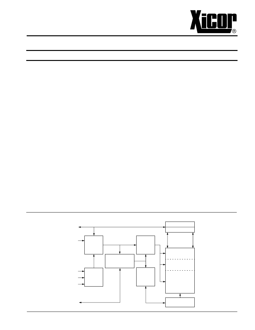
FUNCTIONAL DIAGRAM
FEATURES
Save Critical Data with Programmable
Block Lock Protection
—Block Lock (0, 1/4, 1/2, or all of E
—Software Write Protection
—Programmable Hardware Write Protect
In Circuit Programmable ROM Mode
400KHz 2-Wire Serial Interface
—Schmitt Trigger Input Noise Suppression
—Output Slope Control for Ground Bounce
Noise Elimination
Longer Battery Life With Lower Power
—Active Read Current Less Than 1mA
—Active Write Current Less Than 3mA
—Standby Current Less Than 1
1.8V to 3.6V, 2.5V to 5.5V and 4.5V to 5.5V
Power Supply Versions
32 Word Page Write Mode
—Minimizes Total Write Time Per Word
Internally Organized 4K x 8
Bidirectional Data Transfer Protocol
Self-Timed Write Cycle
—Typical Write Cycle Time of 5ms
High Reliability
—Endurance: 100,000 Cycles
—Data Retention: 100 Years
8-Lead SOIC
14-Lead TSSOP
8-Lead PDIP
2
PROM Array)
μ
A
DESCRIPTION
The X24320 is a CMOS Serial E
organized 4K x 8. The device features a serial inter-
face and software protocol allowing operation on a
simple two wire bus. The bus operates at 400 KHz all
the way down to 1.8V.
2
PROM, internally
Three device select inputs (S
devices to share a common two wire bus.
0
–S
2
) allow up to eight
A Write Protect Register at the highest address loca-
tion, FFFFh, provides three write protection features:
Software Write Protect, Block Lock Protect, and
Programmable Hardware Write Protect. The Software
Write Protect feature prevents any nonvolatile writes to
the device until the WEL bit in the Write Protect
Register is set. The Block Lock Protection feature
gives the user four array block protect options, set by
programming two bits in the Write Protect Register.
The Programmable Hardware Write Protect feature
allows the user to install the device with WP tied to
V
CC
, write to and Block Lock the desired portions of
the memory array in circuit, and then enable the In
Circuit Programmable ROM Mode by programming the
WPEN bit HIGH in the Write Protect Register. After
this, the Block Locked portions of the array, including
the Write Protect Register itself, are permanently
protected from being erased.
SERIAL E
2
PROM DATA
AND ADDRESS (SDA)
SCL
S2
S1
S0
WP
COMMAND
DECODE
AND
CONTROL
LOGIC
BLOCK LOCK AND
WRITE PROTECT
CONTROL LOGIC
DEVICE
SELECT
LOGIC
WRITE
PROTECT
REGISTER
PAGE
DECODE
LOGIC
DATA REGISTER
Y DECODE LOGIC
1K x 8
1K x 8
2K x 8
WRITE VOLTAGE
CONTROL
SERIAL E
2
PROM
ARRAY
4K x 8
7035 FM 01
相關(guān)PDF資料 |
PDF描述 |
|---|---|
| X24320P-1.8 | 400KHz 2-Wire Serial E2PROM with Block Lock |
| X24320PI | 400KHz 2-Wire Serial E2PROM with Block Lock |
| X24320PI-1.8 | 400KHz 2-Wire Serial E2PROM with Block Lock |
| X24320PI-2.5 | 400KHz 2-Wire Serial E2PROM with Block Lock |
| X24320S8 | 400KHz 2-Wire Serial E2PROM with Block Lock |
相關(guān)代理商/技術(shù)參數(shù) |
參數(shù)描述 |
|---|---|
| X24320P-1.8 | 制造商:ICMIC 制造商全稱:IC MICROSYSTEMS 功能描述:400KHz 2-Wire Serial E2PROM with Block Lock |
| X24320P-2.5 | 制造商:ICMIC 制造商全稱:IC MICROSYSTEMS 功能描述:400KHz 2-Wire Serial E2PROM with Block Lock |
| X24320PG | 制造商:ICMIC 制造商全稱:IC MICROSYSTEMS 功能描述:400KHz 2-Wire Serial E2PROM with Block Lock |
| X24320PG-1.8 | 制造商:ICMIC 制造商全稱:IC MICROSYSTEMS 功能描述:400KHz 2-Wire Serial E2PROM with Block Lock |
| X24320PG-2.5 | 制造商:ICMIC 制造商全稱:IC MICROSYSTEMS 功能描述:400KHz 2-Wire Serial E2PROM with Block Lock |
發(fā)布緊急采購(gòu),3分鐘左右您將得到回復(fù)。