- 您現(xiàn)在的位置:買賣IC網(wǎng) > PDF目錄140361 > WV3EG6434S265BD4MF (MICROSEMI CORP-PMG MICROELECTRONICS) 32M X 64 DDR DRAM MODULE, 0.75 ns, DMA200 PDF資料下載
參數(shù)資料
| 型號: | WV3EG6434S265BD4MF |
| 廠商: | MICROSEMI CORP-PMG MICROELECTRONICS |
| 元件分類: | DRAM |
| 英文描述: | 32M X 64 DDR DRAM MODULE, 0.75 ns, DMA200 |
| 封裝: | LEAD FREE, SO-DIMM-200 |
| 文件頁數(shù): | 9/10頁 |
| 文件大小: | 273K |
| 代理商: | WV3EG6434S265BD4MF |
8
White Electronic Designs Corporation (602) 437-1520 www.whiteedc.com
White Electronic Designs
WV3EG6434S-BD4
April 2005
Rev. 0
ADVANCED
White Electronic Designs Corp. reserves the right to change products or specications without notice.
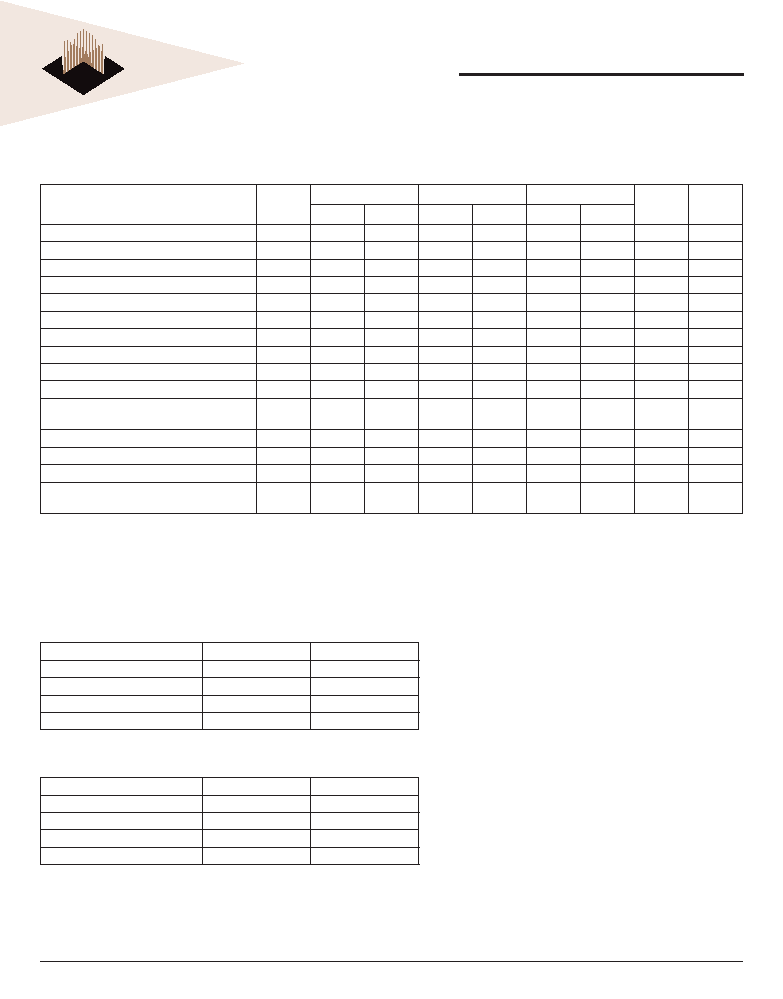
DDR SDRAM COMPONENT ELECTRICAL CHARACTERISTICS AND RECOMMENDED AC
OPERATING CONDITIONS (Continued)
0°C ≤ TA ≤ 70°C, VCC = +2.5V ±0.2V, VCCQ = +2.5V ±0.2V
Parameter
Symbol
335
262
265
Unit
Note
Min
Max
Min
Max
Min
Max
Mode register set cycle time
tMRD
12
15
ns
DQ & DM setup time to DQS
tDS
0.45
0.5
ns
7
DQ & DM hold time to DQS
tDH
0.45
0.5
ns
7
Control & Address input pulse width
tIPW
2.2
ns
DQ & DM input pulse width
tDIPW
1.75
ns
Power down exit time
tPDEX
6
7.5
ns
Exit self refresh to non-Read command
tXSNR
75
ns
4
Exit self refresh to read command
tXSRD
200
tCK
Refresh interval time
tREFI
7.8
us
1
Output DQS valid window
tQH
tHP-tQHS
—tHP-tQHS
—ns
5
Clock half period
tHP
tCLmin or
tCHmin
—
tCLmin or
tCHmin
—
tCLmin or
tCHmin
—ns
Data hold skew factor
tQHS
0.55
0.75
ns
DQS write postamble time
tWPST
0.4
0.6
0.4
0.6
0.4
0.6
tCK
3
Active to Read with Auto precharge command
tRAP
18
20
Autoprecharge write recovery + Precharge
time
tDAL
(tWR/tCK) +
(tRP/tCK)
(tWR/tCK) +
(tRP/tCK)
(tWR/tCK) +
(tRP/tCK)
tCK
1.
Maximum burst refresh cycle : 8
2.
The specic requirement is that DQS be valid(High or Low) on or before this CK edge. The case shown(DQS going from High_Z to logic Low) applies when no writes were
previously in progress on the bus. If a previous write was in progress, DQS could be High at this time, depending on tDQSS.
3.
The maximum limit for this parameter is not a device limit. The device will operate with a great value for this parameter, but system performance (bus turnaround) will degrade
accordingly.
4.
A write command can be applied with tRCD satised after this command.
5.
For registered DIMMs, tCL and tCH are >_ 45% of the period including both the half period jitter (tJIT(HP)) of the PLL and the half period jitter due to crosstalk (tJIT(crosstalk)) on
the DIMM.
6.
Input Setup/Hold Slew Rate Derating
Input Setup/Hold Slew Rate
tIS
tIH
(V/ns)
(ps)
0.5
0
0.4
+50
0.3
+100
This derating table is used to increase tIS/tIH in the case where the input slew rate is below 0.5V/ns. Input setup/hold slew rate based on the lesser of AC-AC slew rate
and DC-DC slew rate.
7.
I/O Setup/Hold Slew Rate Derating
I/O Setup/Hold Slew Rate
tDS
tDH
(V/ns)
(ps)
0.5
0
0.4
+75
0.3
+150
This derating table is used to increase tDS/tDH in the case where the I/O slew rate is below 0.5V/ns. I/O setup/hold slew rate based on the lesser of AC-AC slew rate
and DC-DC slew rate.
相關(guān)PDF資料 |
PDF描述 |
|---|---|
| W1D64M72R8A-3.75AR-JA2 | 64M X 8 DDR DRAM MODULE, 0.5 ns, DMA240 |
| W1D64M72R8A-5AL-HA2 | 64M X 8 DDR DRAM MODULE, 0.5 ns, DMA240 |
| W1D64M72R8A-5AP-QA2 | 64M X 8 DDR DRAM MODULE, 0.5 ns, DMA240 |
| W1D64M72R8A-5AR-JB1 | 64M X 8 DDR DRAM MODULE, 0.5 ns, DMA240 |
| W1D64M72R8B-3.75AE-JA2 | 64M X 8 DDR DRAM MODULE, 0.5 ns, DMA240 |
相關(guān)代理商/技術(shù)參數(shù) |
參數(shù)描述 |
|---|---|
| WV3EG6434S335BD4 | 制造商:WEDC 制造商全稱:White Electronic Designs Corporation 功能描述:256MB - 32Mx64 DDR SDRAM UNBUFFERED, w/PLL |
| WV3EG6434S-BD4 | 制造商:WEDC 制造商全稱:White Electronic Designs Corporation 功能描述:256MB - 32Mx64 DDR SDRAM UNBUFFERED, w/PLL |
| WV3EG6437S335D4IMG | 制造商:WEDC 制造商全稱:White Electronic Designs Corporation 功能描述:256MB - 2x16Mx64 DDR SDRAM SO-DIMM, UNBUFFERED |
| WV3EG6437S335D4ING | 制造商:WEDC 制造商全稱:White Electronic Designs Corporation 功能描述:256MB - 2x16Mx64 DDR SDRAM SO-DIMM, UNBUFFERED |
| WV3EG6437S335D4ISG | 制造商:WEDC 制造商全稱:White Electronic Designs Corporation 功能描述:256MB - 2x16Mx64 DDR SDRAM SO-DIMM, UNBUFFERED |
發(fā)布緊急采購,3分鐘左右您將得到回復。