- 您現(xiàn)在的位置:買賣IC網(wǎng) > PDF目錄361941 > WSF128K32-70H2M 128KX32 SRAM/FLASH MODULE PDF資料下載
參數(shù)資料
| 型號(hào): | WSF128K32-70H2M |
| 英文描述: | 128KX32 SRAM/FLASH MODULE |
| 中文描述: | 128KX32的SRAM /閃存模塊 |
| 文件頁(yè)數(shù): | 1/12頁(yè) |
| 文件大小: | 451K |
| 代理商: | WSF128K32-70H2M |
1
White Electronic Designs Corporation (602) 437-1520 www.wedc.com
White Electronic Designs
WSF128K32-XH2X
October 2004
Rev. 4
White Electronic Designs Corp. reserves the right to change products or specifications without notice.
PRELIMINARY*
128K
X
32 SRAM/FLASH MODULE
FEATURES
Access Times of 25ns (SRAM) and 70, 90 and
120ns (FLASH)
Packaging:
66-pin, PGA Type, 1.385 inch square HIP,
Hermetic Ceramic HIP (Package 402)
128Kx32 SRAM
128Kx32 5V Flash
Organized as 128Kx32 of SRAM and 128Kx32 of
Flash Memory with common Data Bus
Low Power CMOS
Commercial, Industrial and Military Temperature
Ranges
TTL Compatible Inputs and Outputs
Built-in Decoupling Caps and Multiple Ground Pins
for Low Noise Operation
Weight - 13 grams typical
FLASH MEMORY FEATURES
10,000 Erase/Program Cycles
Sector Architecture
8 equal size sectors of 16K bytes each
Any combination of sectors can be concurrently
erased. Also supports full chip erase
5 Volt Programming; 5V ± 10% Supply
Embedded Erase and Program Algorithms
Hardware Write Protection
Page Program Operation and Internal Program
Control Time.
* This product is under development, not fully characterized, and is subject to change
without notice.
Note: Programming information available upon request.
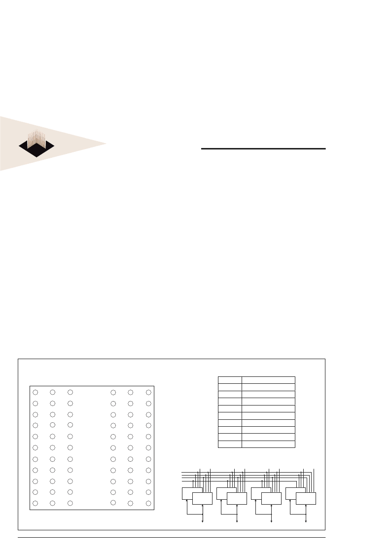
FIGURE 1 – PIN CONFIGURATION FOR WSF128K32-XH2X
Block Diagram
I/O
8
I/O
9
I/O
10
A
14
A
16
A
11
A
0
NC
I/O
0
I/O
1
I/O
2
FWE
2
#
SWE
2
#
GND
I/O
11
A
10
A
9
A
15
V
CC
FCS#
SCS#
I/O
3
I/O
15
I/O
14
I/O
13
I/O
12
OE#
NC
FWE
1
#
I/O
7
I/O
6
I/O
5
I/O
4
I/O
24
I/O
25
I/O
26
A
7
A
12
SWE
1
#
A
13
A
8
I/O
16
I/O
17
I/O
18
V
CC
SWE
4
#
FWE
4
#
I/O
27
A
4
A
5
A
6
FWE
3
#
SWE
3
#
GND
I/O
19
I/O
31
I/O
30
I/O
29
I/O
28
A
1
A
2
A
3
I/O
23
I/O
22
I/O
21
I/O
20
11 22 33 44 55 66
1 12 23 34 45 56
Top View
OE#
A
0-16
FCS#
SCS#
FWE
1
#
SWE
1
#
FWE
2
#
SWE
2
#
FWE
3
#
SWE
3
#
FWE
4
#
SWE
4
#
128K x 8 Flash
128K x 8 SRAM
I/O
0-7
128K x 8 Flash
128K x 8 SRAM
I/O
8-15
128K x 8 Flash
128K x 8 SRAM
I/O
16-23
128K x 8 Flash
128K x 8 SRAM
I/O
24-31
Pin Description
Data Inputs/Outputs
Address Inputs
SWE1-4#
SRAM Write Enable
SCS#
SRAM Chip Selects
OE#
Output Enable
V
CC
Power Supply
GND
Ground
NC
Not Connected
FWE1-4#
Flash Write Enable
FCS#
Flash Chip Select
D0-31
A0-16
相關(guān)PDF資料 |
PDF描述 |
|---|---|
| WSF128K32-70H2MA | 128KX32 SRAM/FLASH MODULE |
| WSF128K32-90H2C | 128KX32 SRAM/FLASH MODULE |
| WSF128K32-90H2CA | 128KX32 SRAM/FLASH MODULE |
| WSF128K32-90H2I | 128KX32 SRAM/FLASH MODULE |
| WSF128K32-90H2IA | 128KX32 SRAM/FLASH MODULE |
相關(guān)代理商/技術(shù)參數(shù) |
參數(shù)描述 |
|---|---|
| WSF128K32-70H2MA | 制造商:WEDC 制造商全稱:White Electronic Designs Corporation 功能描述:128KX32 SRAM/FLASH MODULE |
| WSF128K32-90H2C | 制造商:WEDC 制造商全稱:White Electronic Designs Corporation 功能描述:128KX32 SRAM/FLASH MODULE |
| WSF128K32-90H2CA | 制造商:WEDC 制造商全稱:White Electronic Designs Corporation 功能描述:128KX32 SRAM/FLASH MODULE |
| WSF128K32-90H2I | 制造商:WEDC 制造商全稱:White Electronic Designs Corporation 功能描述:128KX32 SRAM/FLASH MODULE |
| WSF128K32-90H2IA | 制造商:WEDC 制造商全稱:White Electronic Designs Corporation 功能描述:128KX32 SRAM/FLASH MODULE |
發(fā)布緊急采購(gòu),3分鐘左右您將得到回復(fù)。