- 您現(xiàn)在的位置:買賣IC網(wǎng) > PDF目錄361880 > WM8199SCDS (Wolfson Microelectronics) 20MSPS 16-bit CCD Digitiser PDF資料下載
參數(shù)資料
| 型號(hào): | WM8199SCDS |
| 廠商: | Wolfson Microelectronics |
| 英文描述: | 20MSPS 16-bit CCD Digitiser |
| 中文描述: | 20MSPS 16位數(shù)字化儀防治荒漠化公約 |
| 文件頁數(shù): | 13/30頁 |
| 文件大小: | 358K |
| 代理商: | WM8199SCDS |
第1頁第2頁第3頁第4頁第5頁第6頁第7頁第8頁第9頁第10頁第11頁第12頁當(dāng)前第13頁第14頁第15頁第16頁第17頁第18頁第19頁第20頁第21頁第22頁第23頁第24頁第25頁第26頁第27頁第28頁第29頁第30頁
WM8199
Production Data
w
PD Rev 3.2 November 2003
13
TIMING CONTROL
R
S
S/H
4-BIT
RLC DAC
CL
+
+
-
TO OFFSET DAC
RLC
CDS
FROM CONTROL
INTERFACE
S/H
V
S
FROM CONTROL
INTERFACE
MCLK
VSMP
RLC/ACYC
INPUT SAMPLING
BLOCK FOR RED
CHANNEL
CDS
C
IN
RINP
VRLC/
VBIAS
2
1
EXTERNAL VRLC
VRLCEXT
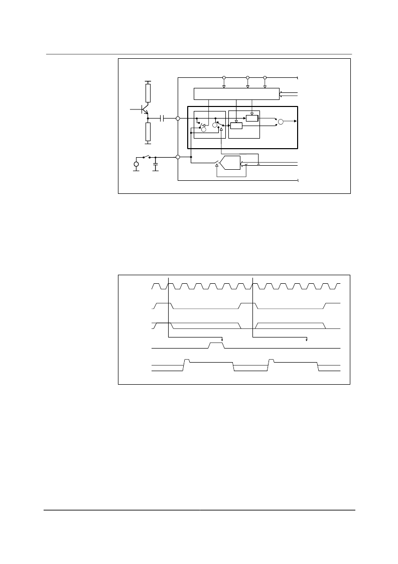
Figure 8 Reset Level Clamping and CDS Circuitry
If auto-cycling is not required, RLC can be selected by pin RLC/ACYC. Figure 9 illustrates control of
RLC for a typical CCD waveform, with CL applied during the reset period.
The input signal applied to the RLC pin is sampled on the positive edge of MCLK that occurs during
each VSMP pulse. The sampled level, high (or low) controls the presence (or absence) of the internal
CL pulse on the next reset level. The position of CL can be adjusted by using control bits
CDSREF[1:0] (Figure 10).
If auto-cycling is required, pin RLC/ACYC is no longer available for this function and control bit
RLCINT determines whether clamping is applied.
Figure 9 Relationship of RLC Pin, MCLK and VSMP to Internal Clamp Pulse, CL
The VRLC/VBIAS pin can be driven internally by a 4-bit DAC (RLCDAC) by writing to control bits
RLCV[3:0]. The RLCDAC range and step size may be increased by writing to control bit
RLCDACRNG. Alternatively, the VRLC/VBIAS pin can be driven externally by writing to control bit
VRLCEXT to disable the RLCDAC and then applying a d.c. voltage to the pin.
CDS/NON-CDS PROCESSING
For CCD type input signals, the signal may be processed using CDS, which will remove pixel-by-pixel
common mode noise. For CDS operation, the video level is processed with respect to the video reset
level, regardless of whether RLC has been performed. To sample using CDS, control bit CDS must
be set to 1 (default), this controls switch 2 (Figure 8) and causes the signal reference to come from
the video reset level. The time at which the reset level is sampled, by clock R
s
/CL, is adjustable by
programming control bits CDSREF[1:0], as shown in Figure 10.
MCLK
VSMP
ACYC/RLC
or RLCINT
CL
(CDSREF = 01)
INPUT VIDEO
1
X
X
0
X
X
0
RGB
RGB
No RLC on this Pixel
RLC on this Pixel
Programmable Delay
RGB
相關(guān)PDF資料 |
PDF描述 |
|---|---|
| WM8716 | High Performance 24-bit, 192kHz Stereo DAC |
| WM8716EDS | High Performance 24-bit, 192kHz Stereo DAC |
| WM8718 | 24 BIT DIFFERENTIAL STEREO DAC WITH VOLUME CONTROL |
| WM8718EDS | 24 BIT DIFFERENTIAL STEREO DAC WITH VOLUME CONTROL |
| WM8718SEDS | 24 BIT DIFFERENTIAL STEREO DAC WITH VOLUME CONTROL |
相關(guān)代理商/技術(shù)參數(shù) |
參數(shù)描述 |
|---|---|
| WM8199SCDS/RV | 功能描述:視頻模擬/數(shù)字化轉(zhuǎn)換器集成電路 16-Bit 20MSPS 3-Channel AFE RoHS:否 制造商:Texas Instruments 輸入信號(hào)類型:Differential 轉(zhuǎn)換器數(shù)量:1 ADC 輸入端數(shù)量:4 轉(zhuǎn)換速率:3 Gbps 分辨率:8 bit 結(jié)構(gòu): 輸入電壓:3.3 V 接口類型:SPI 信噪比: 電壓參考: 電源電壓-最大:3.45 V 電源電壓-最小:3.15 V 最大功率耗散: 最大工作溫度:+ 85 C 最小工作溫度:- 40 C 封裝 / 箱體:TCSP-48 封裝:Reel |
| WM8199SCDS/V | 功能描述:視頻模擬/數(shù)字化轉(zhuǎn)換器集成電路 16-Bit 20MSPS 3-Channel AFE RoHS:否 制造商:Texas Instruments 輸入信號(hào)類型:Differential 轉(zhuǎn)換器數(shù)量:1 ADC 輸入端數(shù)量:4 轉(zhuǎn)換速率:3 Gbps 分辨率:8 bit 結(jié)構(gòu): 輸入電壓:3.3 V 接口類型:SPI 信噪比: 電壓參考: 電源電壓-最大:3.45 V 電源電壓-最小:3.15 V 最大功率耗散: 最大工作溫度:+ 85 C 最小工作溫度:- 40 C 封裝 / 箱體:TCSP-48 封裝:Reel |
| WM8200 | 制造商:WOLFSON 制造商全稱:WOLFSON 功能描述:40MSPS ADC with PGA |
| WM8200-10 | 制造商:WOLFSON 制造商全稱:WOLFSON 功能描述:40MSPS ADC with PGA |
| WM8200-10IFL | 制造商:WOLFSON 制造商全稱:WOLFSON 功能描述:40MSPS ADC with PGA |
發(fā)布緊急采購,3分鐘左右您將得到回復(fù)。