- 您現(xiàn)在的位置:買賣IC網(wǎng) > PDF目錄361880 > WM8181 (Wolfson Microelectronics) 12-bit 2MSPS Serial Output CIS/CCD Digitiser PDF資料下載
參數(shù)資料
| 型號: | WM8181 |
| 廠商: | Wolfson Microelectronics |
| 英文描述: | 12-bit 2MSPS Serial Output CIS/CCD Digitiser |
| 中文描述: | 12位2MSPS串行輸出獨聯(lián)體/防治荒漠化公約數(shù)字化儀 |
| 文件頁數(shù): | 8/14頁 |
| 文件大小: | 150K |
| 代理商: | WM8181 |
WM8181
Advanced Information
WOLFSON MICROELECTRONICS LTD
AI Rev 3.0 January 2000
8
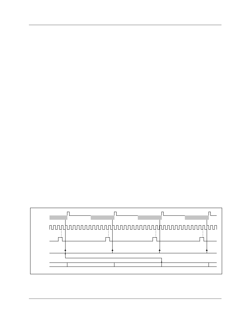
OVERALL TIMING
The WM8181 input sampling, conversion and data output is controlled by externally applied MCLK
and VSMP clocks. Please refer to the Operational Timing Diagrams (Figures 4 and 5) shown at the
end of this section.
12:1 MCLK: VSMP RATIO OPERATION
MCLK can run at speeds of up to 24MHz. VSMP is a pulse one MCLK period long, with 12 times the
period of MCLK. VSMP must cover one rising edge of MCLK.
If VSMP is high for more than one MCLK rising edge, the last MCLK rising edge that is covered is
defined as the starting point and the video signal will be sampled on the next rising edge of MCLK.
Output data being processed at this time may be corrupted.
VSMP should be held low for 11 MCLK rising edges, then pulsed high for the 12th MCLK rising edge
to produce an MCLK:VSMP ratio of 12:1. If VSMP is held low for less than 11 MCLK rising edges,
the device will reset to the starting point and the video signal will be sampled on the next rising edge
of MCLK. Output data being processed during this time may be corrupted.
16:1 MCLK: VSMP RATIO OPERATION
The WM8181 can also operate with an MCLK:VSMP ratio of 16:1. Video signal sampling is
performed in the same manner as in 12:1 operation except that the device will wait an extra four
MCLK periods for the next VSMP pulse to go low before sampling the video signal.
DEVICE LATENCY
For 12:1 operation, the WM8181 will start to output valid data MSB first on the falling edge of MCLK
24.5 MCLK periods after the sampling instant (first rising edge of MCLK after VSMP goes low) for
that pixel. The device continues to output the data on the next 11 falling edges of MCLK
For 16:1 operation, the output latency increases to 32.5 MCLK periods after the sampling instant.
Data is output MSB first on this falling edge of MCLK, and continues over the next 11 falling edges of
MCLK. The four bits between the end of one output and the start of the next will be 0.
POWER DOWN
If VSMP is held high for 64 MCLK rising edges, the device will power down, causing DOUT, VRT,
and VRB to change into a high impedance state. The device will start powering up immediately on
VSMP going low, however VRT and VRB will take some time to recover and settle, depending on
how their voltages have decayed during power down and the decoupling capacitors used. Typically
for 1
μ
F decoupling capacitors the amount of time taken for VRT and VRB to recover may be up to
10ms. If 0.1
μ
F capacitors are used, this time will decrease to typically 1ms.
OPERATIONAL TIMING DIAGRAMS
CCD
Outputs
VSMP
S/H
Reset
DOUT
MCLK
Reset
Video Pixel 1
Reset
Video Pixel 2
Video Pixel 3
D11
→
D0 PIXEL - 2
D11
→
D0 PIXEL - 1
D11
→
D0 PIXEL 0
LATENCY = 24.5 MCLK PERIODS
Video Pixel 0
Figure 4 12:1 Operation
相關(guān)PDF資料 |
PDF描述 |
|---|---|
| WM8190 | TVS UNIDIRECT 6V 400W SMA |
| WM8191 | TVS BI-DIR 6.0V 400W SMA |
| WM8192 | TVS UNIDIRECT 400W 6.5V SMA |
| WM8196 | (8+8)BIT OUTPUT 16-BIT CIS/CCD AFE/DIGITISER |
| WM8199 | 20MSPS 16-bit CCD Digitiser |
相關(guān)代理商/技術(shù)參數(shù) |
參數(shù)描述 |
|---|---|
| WM8190 | 制造商:WOLFSON 制造商全稱:WOLFSON 功能描述:(8+6) Bit Output 14-bit CIS/CCD AFE/Digitiser |
| WM8191 | 制造商:WOLFSON 制造商全稱:WOLFSON 功能描述:14-bit 6MSPS CIS/CCD Analogue Front End/Digitiser |
| WM8192 | 制造商:WOLFSON 制造商全稱:WOLFSON 功能描述:(8+8) Bit Output 16-bit CIS/CCD AFE/Digitiser |
| WM8195 | 制造商:WOLFSON 制造商全稱:WOLFSON 功能描述:14-bit 12MSPS CIS/CCD Analogue Front End/Digitiser |
| WM8195_05 | 制造商:WOLFSON 制造商全稱:WOLFSON 功能描述:14-bit 12MSPS CIS/CCD Analogue Front End/Digitiser |
發(fā)布緊急采購,3分鐘左右您將得到回復(fù)。