- 您現(xiàn)在的位置:買賣IC網(wǎng) > PDF目錄202142 > WED9LC6816V1610BI (WHITE ELECTRONIC DESIGNS CORP) SPECIALTY MEMORY CIRCUIT, PBGA153 PDF資料下載
參數(shù)資料
| 型號: | WED9LC6816V1610BI |
| 廠商: | WHITE ELECTRONIC DESIGNS CORP |
| 元件分類: | 存儲器 |
| 英文描述: | SPECIALTY MEMORY CIRCUIT, PBGA153 |
| 封裝: | 14 X 22 MM, MO-163, BGA-153 |
| 文件頁數(shù): | 22/26頁 |
| 文件大小: | 324K |
| 代理商: | WED9LC6816V1610BI |
第1頁第2頁第3頁第4頁第5頁第6頁第7頁第8頁第9頁第10頁第11頁第12頁第13頁第14頁第15頁第16頁第17頁第18頁第19頁第20頁第21頁當(dāng)前第22頁第23頁第24頁第25頁第26頁
WED9LC6816V
5
White Electronic Designs Corporation (602) 437-1520 www.whiteedc.com
White Electronic Designs
September, 2003
Rev. 1
White Electronic Designs Corp. reserves the right to change products or specications without notice.
BGA CAPACITANCE
NOTE:
1.
This parameter is sampled.
(VCC = 3.3V -5% / +10% unless otherwise noted; 0°C tA 70°C, Commercial; -40°C tA 85°C, Industrial)
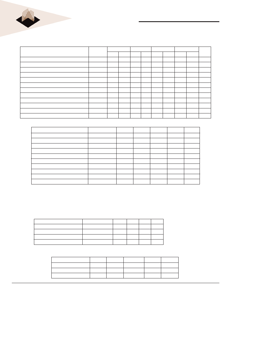
SSRAM AC CHARACTERISTICS
Parameter
Symbol
200MHz
166MHz
150MHz
133MHz
Units
Min
Max
Min
Max
Min
Max
Min
Max
Clock Cycle Time
tKHKH
56
7
8
ns
Clock HIGH Time
tKLKH
1.6
2.4
2.6
2.8
ns
Clock LOW Time
tKHKL
1.6
2.4
2.6
2.8
ns
Clock to output valid
tKHQV
2.5
3.5
3.8
4.0
ns
Clock to output invalid
tKHQX
1.5
ns
Clock to output on Low-Z
tKQLZ
00
0
ns
Clock to output in High-Z
tKQHZ
1.5
3
1.5
3.5
1.5
3.8
1.5
4.0
ns
Output Enable to output valid
tOELQV
2.5
3.5
3.8
4.0
ns
Output Enable to output in Low-Z
tOELZ
00
0
ns
Output Enable to output in High-Z
tOEHZ
3.0
3.5
3.8
ns
Address, Control, Data-in Setup Time to Clock
tS
1.5
ns
Address, Control, Data-in Hold Time to Clock
tH
0.5
ns
Description
Conditions
Symbol
Typ
Max
Units
Address Input Capacitance (1)
tA = 25°C; f = 1MHz
CI
5
8
pF
Input/Output Capacitance (DQ) (1)
tA = 25°C; f = 1MHz
CO
8
10
pF
Control Input Capacitance (1)
tA = 25°C; f = 1MHz
CA
5
8
pF
Clock Input Capacitance (1)
tA = 25°C; f = 1MHz
CCK
4
6
pF
SSRAM OPERATION TRUTH TABLE
NOTE:
1.
X means “don’t care”, H means logic HIGH. L means logic LOW.
2.
All inputs except SSOE# must meet setup and hold times around the rising edge (LOW to HIGH) of SSCK.
3.
Suspending burst generates wait cycle
4.
For a write operation following a read operation, SSOE# must be HIGH before the input data required setup time plus High-Z
time for SSOE# and staying HIGH through out the input data hold time.
5.
This device contains circuitry that will ensure the outputs will be in High-Z during power-up.
SSRAM PARTIAL TRUTH TABLE
Function
SSWE#
BWE0#
BWE1#
BWE2#
BWE3#
READ
H
X
WRITE one Byte (DQ0-7)
L
H
WRITE all Bytes
L
Operation
Address Used
SSCE#
SSADS#
SSWE#
SSOE#
DQ
Deselected Cycle, Power Down
None
H
L
X
High-Z
WRITE Cycle, Begin Burst
External
L
X
D
READ Cycle, Begin Burst
External
L
H
L
Q
READ Cycle, Begin Burst
External
L
H
High-Z
READ Cycle, Suspend Burst
Current
X
H
L
Q
READ Cycle, Suspend Burst
Current
X
H
High-Z
READ Cycle, Suspend Burst
Current
H
L
Q
READ Cycle, Suspend Burst
Current
H
High-Z
WRITE Cycle, Suspend Burst
Current
X
H
L
X
D
WRITE Cycle, Suspend Burst
Current
H
L
X
D
相關(guān)PDF資料 |
PDF描述 |
|---|---|
| WS128K32V-20G2TIA | 128K X 32 MULTI DEVICE SRAM MODULE, 20 ns, CQMA68 |
| W3EG2128M64ETSR335JD3SG | 256M X 64 DDR DRAM MODULE, 0.7 ns, DMA184 |
| W3DG6463V7D2-GG | 64M X 64 SYNCHRONOUS DRAM MODULE, 5.4 ns, DMA168 |
| WED3DG644V75D1I-MG | 4M X 64 SYNCHRONOUS DRAM MODULE, ZMA144 |
| W3HG2256M72ACER534D6MG | 512M X 72 DDR DRAM MODULE, 0.5 ns, DMA240 |
相關(guān)代理商/技術(shù)參數(shù) |
參數(shù)描述 |
|---|---|
| WED9LC6816V1612BC | 制造商:未知廠家 制造商全稱:未知廠家 功能描述:256K X 32 SSRAM/ 4M X 32 SDRAM |
| WED9LC6816V1612BI | 制造商:未知廠家 制造商全稱:未知廠家 功能描述:256K X 32 SSRAM/ 4M X 32 SDRAM |
| WED9LC6816V2010BC | 制造商:未知廠家 制造商全稱:未知廠家 功能描述:256K X 32 SSRAM/ 4M X 32 SDRAM |
| WED9LC6816V2010BI | 制造商:未知廠家 制造商全稱:未知廠家 功能描述:256K X 32 SSRAM/ 4M X 32 SDRAM |
| WED9LC6816V2012BC | 制造商:未知廠家 制造商全稱:未知廠家 功能描述:256K X 32 SSRAM/ 4M X 32 SDRAM |
發(fā)布緊急采購,3分鐘左右您將得到回復(fù)。