- 您現(xiàn)在的位置:買賣IC網(wǎng) > PDF目錄202124 > WE32K32N-80H1CA (WHITE ELECTRONIC DESIGNS CORP) 32K X 32 EEPROM 5V MODULE, 80 ns, CPGA66 PDF資料下載
參數(shù)資料
| 型號: | WE32K32N-80H1CA |
| 廠商: | WHITE ELECTRONIC DESIGNS CORP |
| 元件分類: | PROM |
| 英文描述: | 32K X 32 EEPROM 5V MODULE, 80 ns, CPGA66 |
| 封裝: | 1.075 X 1.075 INCH, HERMETIC SEALED, CERAMIC, HIP-66 |
| 文件頁數(shù): | 8/13頁 |
| 文件大?。?/td> | 533K |
| 代理商: | WE32K32N-80H1CA |
4
White Electronic Designs Corporation (602) 437-1520 www.whiteedc.com
White Electronic Designs
WE32K32-XXX
March 2006
Rev. 4
White Electronic Designs Corp. reserves the right to change products or specications without notice.
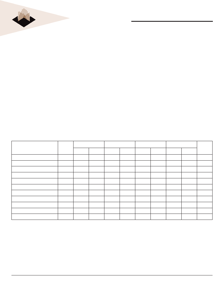
AC Write Characteristics
VCC = 5.0V, GND = 0V, -55°C ≤ TA ≤ +125°C
WRITE CYCLE
Write Cycle Parameter
Symbol
-80
-90
-120
-150
Unit
Min
Max
Min
Max
Min
Max
Min
Max
Write Cycle Time, TYP = 6ms
tWC
10
ms
Address Set-up Time
tAS
0
30
ns
Write Pulse Width (WE# or CS#)
tWP
100
150
ns
Chip Select Set-up Time
tCS
0000
ns
Address Hold Time
tAH
50
100
ns
Data Hold Time
tDH
0
10
ns
Chip Select Hold Time
tCSH
0000
ns
Data Set-up Time
tDS
50
100
ns
Write Pulse Width High
tWPH
50
ns
Output Enable Set-up Time
tOES
10
ns
Output Enable Hold Time
tOEH
10
ns
WRITE
A write cycle is initiated when OE# is high and a low pulse
is on WE# or CS# with CS# or WE# low. The address
is latched on the falling edge of CS# or WE# whichever
occurs last. The data is latched by the rising edge of CS#
or WE#, whichever occurs rst. A byte write operation will
automatically continue to completion.
WRITE CYCLE TIMING
Figures 4 and 5 show the write cycle timing relationships.
A write cycle begins with address application, write enable
and chip select. Chip select is accomplished by placing
the CS# line low. Write enable consists of setting the WE#
line low. The write cycle begins when the last of either CS#
or WE# goes low.
The WE# line transition from high to low also initiates
an internal 150 μsec delay timer to permit page mode
operation. Each subsequent WE# transition from high to
low that occurs before the completion of the 150 μsec time
out will restart the timer from zero. The operation of the
timer is the same as a retriggerable one-shot.
相關PDF資料 |
PDF描述 |
|---|---|
| WE32K32N-120H1IA | 32K X 32 EEPROM 5V MODULE, 120 ns, CPGA66 |
| WS512K32N-17H2MA | 2M X 8 MULTI DEVICE SRAM MODULE, 17 ns, CPGA66 |
| WS512K32N-25H2M | 2M X 8 MULTI DEVICE SRAM MODULE, 25 ns, CPGA66 |
| WME128K8-150CQ | 128K X 8 EEPROM 5V, 150 ns, CDIP32 |
| WMS256K16-20FGC | 256K X 16 STANDARD SRAM, 20 ns, CDSO44 |
相關代理商/技術參數(shù) |
參數(shù)描述 |
|---|---|
| WE32K32N-80H1I | 制造商:未知廠家 制造商全稱:未知廠家 功能描述:EEPROM |
| WE32K32N-80H1IA | 制造商:未知廠家 制造商全稱:未知廠家 功能描述:EEPROM |
| WE32K32N-80H1M | 制造商:未知廠家 制造商全稱:未知廠家 功能描述:EEPROM |
| WE32K32N-80H1MA | 制造商:未知廠家 制造商全稱:未知廠家 功能描述:EEPROM |
| WE32K32N-80H1Q | 制造商:未知廠家 制造商全稱:未知廠家 功能描述:EEPROM |
發(fā)布緊急采購,3分鐘左右您將得到回復。