- 您現(xiàn)在的位置:買賣IC網(wǎng) > PDF目錄68460 > W78M32V120BM (WHITE ELECTRONIC DESIGNS CORP) 8M X 32 FLASH 3.3V PROM, 120 ns, PBGA159 PDF資料下載
參數(shù)資料
| 型號: | W78M32V120BM |
| 廠商: | WHITE ELECTRONIC DESIGNS CORP |
| 元件分類: | PROM |
| 英文描述: | 8M X 32 FLASH 3.3V PROM, 120 ns, PBGA159 |
| 封裝: | 13 X 22 MM, 1.27 MM PITCH, PLASTIC, BGA-159 |
| 文件頁數(shù): | 30/54頁 |
| 文件大?。?/td> | 789K |
| 代理商: | W78M32V120BM |
第1頁第2頁第3頁第4頁第5頁第6頁第7頁第8頁第9頁第10頁第11頁第12頁第13頁第14頁第15頁第16頁第17頁第18頁第19頁第20頁第21頁第22頁第23頁第24頁第25頁第26頁第27頁第28頁第29頁當(dāng)前第30頁第31頁第32頁第33頁第34頁第35頁第36頁第37頁第38頁第39頁第40頁第41頁第42頁第43頁第44頁第45頁第46頁第47頁第48頁第49頁第50頁第51頁第52頁第53頁第54頁
36
White Electronic Designs Corporation (602) 437-1520 www.whiteedc.com
White Electronic Designs
W78M32V-XBX
April 2006
Rev. 3
White Electronic Designs Corp. reserves the right to change products or specications without notice.
WRITE OPERATION STATUS
The device provides several bits to determine the status of
a program or erase operation: DQ2, DQ3, DQ5, DQ6, and
DQ7. Table 15 and the following subsections describe the
function of these bits. DQ7 and DQ6 each offer a method
for determining whether a program or erase operation
is complete or in progress. The device also provides a
hardware-based output signal, RY/BY#, to determine
whether an Embedded Program or Erase operation is in
progress or has been completed.
DQ7: DATA# POLLING
The Data# Polling bit, DQ7, indicates to the host system
whether an Embedded Program or Erase algorithm is
in progress or completed, or whether a bank is in Erase
Suspend. Data# Polling is valid after the rising edge of the
nal WE# pulse in the command sequence.
During the Embedded Program algorithm, the device
outputs on DQ7 the complement of the datum programmed
to DQ7. This DQ7 status also applies to programming during
Erase Suspend. When the Embedded Program algorithm
is complete, the device outputs the datum programmed to
DQ7. The system must provide the program address to read
valid status information on DQ7. If a program address falls
within a protected sector, Data# Polling on DQ7 is active
for approximately 1 μs, then that bank returns to the read
mode.
During the Embedded Erase algorithm, Data# Polling
produces a “0” on DQ7. When the Embedded Erase
algorithm is complete, or if the bank enters the Erase
Suspend mode, Data# Polling produces a “1” on DQ7. The
system must provide an address within any of the sectors
selected for erasure to read valid status information on
DQ7.
After an erase command sequence is written, if all sectors
selected for erasing are protected, Data# Polling on DQ7
is active for approximately 400 μs, then the bank returns
to the read mode. If not all selected sectors are protected,
the Embedded Erase algorithm erases the unprotected
sectors, and ignores the selected sectors that are protected.
However, if the system reads DQ7 at an address within a
protected sector, the status may not be valid.
When the system detects DQ7 has changed from
the complement to true data, it can read valid data at
DQ15–DQ0 on the following read cycles. Just prior to the
completion of an Embedded Program or Erase operation,
DQ7 may change asynchronously with DQ15–DQ0 while
Output Enable (OE#) is asserted low. That is, the device
may change from providing status information to valid data
on DQ7. Depending on when the system samples the
DQ7 output, it may read the status or valid data. Even if
the device has completed the program or erase operation
and DQ7 has valid data, the data outputs on DQ15–DQ0
may be still invalid. Valid data on DQ15–DQ0 will appear
on successive read cycles.
Table 15 shows the outputs for Data# Polling on DQ7.
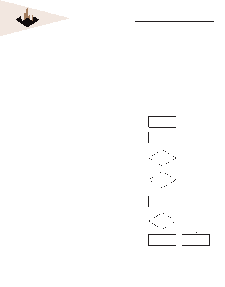
Figure 8 shows the Data# Polling algorithm. Figure 19
in the AC Characteristic section shows the Data# Polling
timing diagram.
DQ7 = Data?
Yes
No
DQ5=1?
No
Yes
PASS
Read DQ7–DQ0
Addr=VA
Read DQ7–DQ0
Addr = VA
DQ7 = Data?
START
FAIL
Notes:
1.
VA = Valid address for programming. During a sector erase operation, a valid address
is any sector address within the sector being erased. During chip erase, a valid
address is any non-protected sector address.
2.
DQ7 should be rechecked even if DQ5 = “1” because DQ7 may change
simultaneously with DQ5.
FIGURE 8. DATA# POLLING ALGORITHM
相關(guān)PDF資料 |
PDF描述 |
|---|---|
| W78M32V90BM | 8M X 32 FLASH 3.3V PROM, 90 ns, PBGA159 |
| W78M32V70BC | 8M X 32 FLASH 3.3V PROM, 70 ns, PBGA159 |
| W78M32VP110BC | 8M X 32 FLASH 3.3V PROM, 110 ns, PBGA159 |
| W78M32VP110BM | 8M X 32 FLASH 3.3V PROM, 110 ns, PBGA159 |
| W78M64V-120SBC | 8M X 64 FLASH 3.3V PROM MODULE, 120 ns, PBGA159 |
相關(guān)代理商/技術(shù)參數(shù) |
參數(shù)描述 |
|---|---|
| W78M32V70BC | 制造商:WEDC 制造商全稱:White Electronic Designs Corporation 功能描述:8Mx32 Flash 3.3V Page Mode Simultaneous Read/Write Operation Multi-Chip Package |
| W78M32V70BI | 制造商:WEDC 制造商全稱:White Electronic Designs Corporation 功能描述:8Mx32 Flash 3.3V Page Mode Simultaneous Read/Write Operation Multi-Chip Package |
| W78M32V70BM | 制造商:WEDC 制造商全稱:White Electronic Designs Corporation 功能描述:8Mx32 Flash 3.3V Page Mode Simultaneous Read/Write Operation Multi-Chip Package |
| W78M32V90BC | 制造商:WEDC 制造商全稱:White Electronic Designs Corporation 功能描述:8Mx32 Flash 3.3V Page Mode Simultaneous Read/Write Operation Multi-Chip Package |
| W78M32V90BI | 制造商:WEDC 制造商全稱:White Electronic Designs Corporation 功能描述:8Mx32 Flash 3.3V Page Mode Simultaneous Read/Write Operation Multi-Chip Package |
發(fā)布緊急采購,3分鐘左右您將得到回復(fù)。