- 您現(xiàn)在的位置:買賣IC網 > PDF目錄68459 > W49F002U-90BN (WINBOND ELECTRONICS CORP) 256K X 8 FLASH 5V PROM, 90 ns, PDIP32 PDF資料下載
參數(shù)資料
| 型號: | W49F002U-90BN |
| 廠商: | WINBOND ELECTRONICS CORP |
| 元件分類: | PROM |
| 英文描述: | 256K X 8 FLASH 5V PROM, 90 ns, PDIP32 |
| 封裝: | PLASTIC, DIP-32 |
| 文件頁數(shù): | 25/27頁 |
| 文件大小: | 233K |
| 代理商: | W49F002U-90BN |
第1頁第2頁第3頁第4頁第5頁第6頁第7頁第8頁第9頁第10頁第11頁第12頁第13頁第14頁第15頁第16頁第17頁第18頁第19頁第20頁第21頁第22頁第23頁第24頁當前第25頁第26頁第27頁
W49F002U
Publication Release Date: February 21, 2002
- 7 -
Revision A6
For chip erase, the Data Polling is valid after the rising edge of the sixth pulse in the six #WE write
pulse sequence. For sector erase, the Data Polling is valid after the last rising edge of the sector erase
#WE pulse.
Just prior to the completion of Embedded Algorithm operations DQ7 may change asynchronously while
the output enable (#OE) is asserted low. This means that the device is driving status information on
DQ7 at one instant of time and then that byte
′s valid data at the next instant of time. Depending on
when the system samples the DQ7 output, it may read the status or valid data. Even if the device has
completed the Embedded Algorithm operations and DQ7 has a valid data, the data outputs on DQ0 –
DQ6 may be still invalid. The valid data on DQ0
DQ7 will be read on the successive read attempts.
The Data Polling feature is only active during the Embedded Programming Algorithm, Embedded
Erase Algorithm, or sector erase time-out (see "Command Definitions").
See " #DATA Polling During Embedded Algorithm Timing Diagrams".
DQ6: Toggle Bit
The W49F002U also features the "Toggle Bit" as a method to indicate to the host system that the
embedded algorithms are in progress or completed.
During an Embedded Program or Erase Algorithm cycle, successive attempts to read (#OE toggling)
data from the device at any address will result in DQ6 toggling between one and zero. Once the
Embedded Program or Erase Algorithm cycle is completed, DQ6 will stop toggling and valid data will
be read on the next successive attempt. During programming, the Toggle Bit is valid after the rising
edge of the fourth #WE pulse in the four write pulse sequence. For chip erase, the Toggle Bit is valid
after the rising edge of the sixth #WE pulse in the six write pulse sequence. For Sector erase, the
Toggle Bit is valid after the last rising edge of the sector erase #WE pulse. The Toggle Bit is active
during the sector erase time-out.
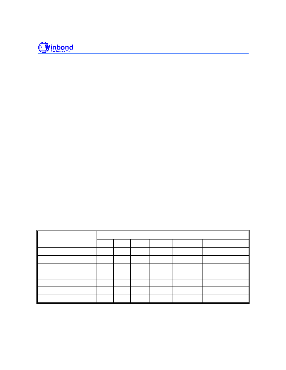
TABLE OF OPERATING MODES
Device Bus Operations
MODE
PIN
#CE
#OE
#WE
#RESET
A0
A17
DQ0
DQ7
Read
VIL
VIH
Ain
Dout
Write
VIL
VIH
VIL
VIH
Ain
Din
Write Inhibit
VIH
X
VIL
X
High Z/DOUT
VIH
X
VIH
X
High Z/DOUT
Standby
VIH
X
VIH
X
High Z
Output Disable
VIL
VIH
X
High Z
Reset
X
VIL
X
High Z
相關PDF資料 |
PDF描述 |
|---|---|
| W49F002UT12N | 256K X 8 FLASH 5V PROM, 120 ns, PDSO32 |
| W55F10B | 1M X 1 FLASH 5V PROM, PDIP8 |
| W6692ACD | DATACOM, ISDN CONTROLLER, PQFP100 |
| W6692ACF | DATACOM, ISDN CONTROLLER, PQFP100 |
| W6694ACD | DATACOM, ISDN CONTROLLER, PQFP48 |
相關代理商/技術參數(shù) |
參數(shù)描述 |
|---|---|
| W49F002UP12B | 制造商:WINBOND 制造商全稱:Winbond 功能描述:256K X 8 CMOS FLASH MEMORY |
| W49F002UP70B | 制造商:WINBOND 制造商全稱:Winbond 功能描述:256K X 8 CMOS FLASH MEMORY |
| W49F002UP90B | 制造商:WINBOND 制造商全稱:Winbond 功能描述:256K X 8 CMOS FLASH MEMORY |
| W49F002UT12B | 制造商:WINBOND 制造商全稱:Winbond 功能描述:256K X 8 CMOS FLASH MEMORY |
| W49F002UT70B | 制造商:WINBOND 制造商全稱:Winbond 功能描述:256K X 8 CMOS FLASH MEMORY |
發(fā)布緊急采購,3分鐘左右您將得到回復。