- 您現(xiàn)在的位置:買賣IC網(wǎng) > PDF目錄68457 > W3HG2128M64EEU534XD4MG (MICROSEMI CORP-PMG MICROELECTRONICS) SYNCHRONOUS DRAM MODULE, DMA200 PDF資料下載
參數(shù)資料
| 型號: | W3HG2128M64EEU534XD4MG |
| 廠商: | MICROSEMI CORP-PMG MICROELECTRONICS |
| 元件分類: | DRAM |
| 英文描述: | SYNCHRONOUS DRAM MODULE, DMA200 |
| 封裝: | ROHS COMPLIANT, SODIMM-200 |
| 文件頁數(shù): | 12/13頁 |
| 文件大小: | 188K |
| 代理商: | W3HG2128M64EEU534XD4MG |
W3HG2128M64EEU-D4
January 2008
Rev. 7
8
White Electronic Designs Corporation (602) 437-1520 www.whiteedc.com
White Electronic Designs
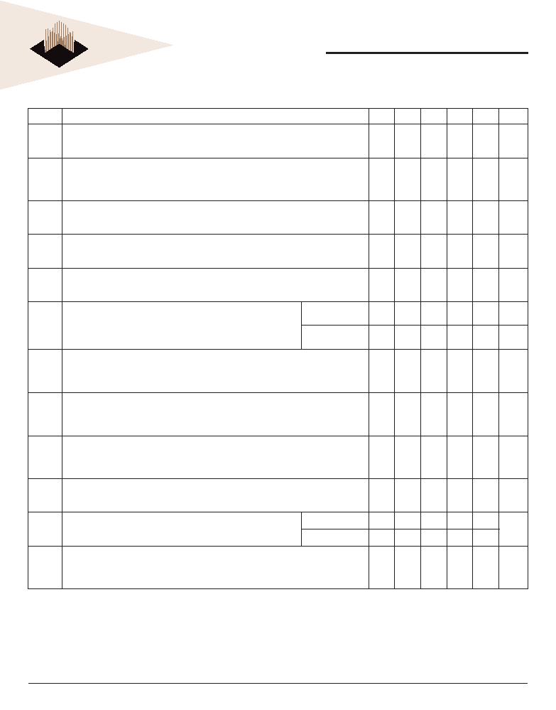
DDR2 ICC SPECIFICATION
Symbol
Proposed Conditions
805
806
665
534
403
Units
ICC0*
Operating one bank active-precharge;
tCK = tCK(ICC), tRC = tRC(ICC), tRAS = tRAS min(ICC); CKE is HIGH, CS# is HIGH between valid commands;
Address bus inputs are SWITCHING; Data bus inputs are SWITCHING
776
736
616
mA
ICC1*
Operating one bank active-read-precharge;
IOUT = 0mA; BL = 4, CL = CL(ICC), AL = 0; tCK = tCK(ICC), tRC = tRC (ICC), tRAS = tRAS min(ICC); CKE is
HIGH, CS# is HIGH between valid commands; Address bus inputs are SWITCHING; Data pattern is
same as ICC4W
936
856
816
776
mA
ICC2P**
Precharge power-down current;
All banks idle; tCK = tCK(ICC); CKE is LOW; Other control and address bus inputs are STABLE; Data bus
inputs are FLOATING
112
mA
ICC2Q**
Precharge quiet standby current;
All banks idle; tCK = tCK(ICC); CKE is HIGH, CS# is HIGH; Other control and address bus inputs are
STABLE; Data bus inputs are FLOATING
800
640
560
mA
ICC2N**
Precharge standby current;
All banks idle; tCK = tCK(ICC); CKE is HIGH, CS# is HIGH; Other control and address bus inputs are
STABLE; Data bus inputs are SWITCHING
800
640
560
mA
ICC3P**
Active power-down current;
All banks open; tCK = tCK(ICC); CKE is LOW; Other control and address bus
inputs are STABLE; Data bus inputs are FLOATING
Fast PDN Exit
MRS(12) = 0
800
480
mA
Slow PDN Exit
MRS(12) = 1
160
mA
ICC3N**
Active standby current;
All banks open; tCK = tCK(ICC), tRC = tRC(ICC, tRAS = tRAS min(ICC); CKE is HIGH, CS# is HIGH between
valid commands; Other control and address bus inputs are SWITCHING; Data bus inputs are
SWITCHING
960
880
720
640
mA
ICC4W*
Operating burst write current;
All banks open, Continuous burst writes; BL = 4, CL = CL(ICC), AL = 0; tCK = tCK(ICC), tRAS =
tRASmax(ICC), tRP = tRP(ICC); CKE is HIGH, CS# is HIGH between valid commands; Address bus inputs
are SWITCHING; Data bus inputs are SWITCHING
1,336
1,136
1,056
896
mA
ICC4R*
Operating burst read current;
All banks open, Continuous burst reads, IOUT = 0mA; BL = 4, CL = CL(ICC), AL = 0; tCK = tCK(ICC), tRAS =
tRASmax(ICC), tRP = tRP(ICC); CKE is HIGH, CS# is HIGH between valid commands; Address bus inputs
are SWITCHING; Data pattern is same as ICC4W
1,336
1,136
1,056
896
mA
ICC5**
Burst auto refresh current;
tCK = tCK(ICC); Refresh command at every tRFC(ICC) interval; CKE is HIGH, CS# is HIGH between valid
commands; Other control and address bus inputs are SWITCHING; Data bus inputs are SWITCHING
3,760
3,440
3,360
3,280
mA
ICC6**
Self refresh current;
CK and CK# at 0V; CKE 0.2V; Other control and address bus inputs are
FLOATING; Data bus inputs are FLOATING
Normal
112
mA
Low Power
80
ICC7*
Operating bank interleave read current;
All bank interleaving reads, IOUT = 0mA; BL = 4, CL = CL(ICC), AL = tRCD(ICC)-1*tCK(ICC); tCK = tCK(ICC),
tRC = tRC(ICC), tRRD = tRRD(ICC), tRCD = 1*tCK(ICC); CKE is HIGH, CS# is HIGH between valid commands;
Address bus inputs are STABLE during DESELECTs; Data bus inputs are SWITCHING.
2,736
2,296
2,216
2,136
mA
ICC specication is based on
MICRON (1G E-die revision) components. Other DRAM manufactures specication may be different.
Note:
* Value calculated as one module rank in this operating condition, and all other module ranks in ICC2P (CKE LOW) mode.
** Value calculated reects all module ranks in this operating condition.
相關PDF資料 |
PDF描述 |
|---|---|
| W3HG2128M64EEU806D4ISG | 256M X 64 DDR DRAM MODULE, 0.4 ns, DMA200 |
| W3HG2128M72ACER534AD6MG | 256M X 72 DDR DRAM MODULE, 0.5 ns, DMA240 |
| W3HG2128M72ACER806AD6IMG | 256M X 72 DDR DRAM MODULE, DMA240 |
| W3HG2128M72ACER534AD6IMG | 256M X 72 DDR DRAM MODULE, 0.5 ns, DMA240 |
| W3HG2128M72ACER806AD6IMG | 256M X 72 DDR DRAM MODULE, DMA240 |
相關代理商/技術參數(shù) |
參數(shù)描述 |
|---|---|
| W3HG2128M72ACER403AD6XG | 制造商:WEDC 制造商全稱:White Electronic Designs Corporation 功能描述:2GB - 2x128Mx72 DDR2 SDRAM REGISTERED, w/PLL, VLP |
| W3HG2128M72ACER534AD6XG | 制造商:WEDC 制造商全稱:White Electronic Designs Corporation 功能描述:2GB - 2x128Mx72 DDR2 SDRAM REGISTERED, w/PLL, VLP |
| W3HG2128M72ACER665AD6XG | 制造商:WEDC 制造商全稱:White Electronic Designs Corporation 功能描述:2GB - 2x128Mx72 DDR2 SDRAM REGISTERED, w/PLL, VLP |
| W3HG2128M72ACER806AD6XG | 制造商:WEDC 制造商全稱:White Electronic Designs Corporation 功能描述:2GB - 2x128Mx72 DDR2 SDRAM REGISTERED, w/PLL, VLP |
| W3HG2128M72ACER-AD6 | 制造商:WEDC 制造商全稱:White Electronic Designs Corporation 功能描述:2GB - 2x128Mx72 DDR2 SDRAM REGISTERED, w/PLL, VLP |
發(fā)布緊急采購,3分鐘左右您將得到回復。